LED chip capable of improving light-discharging rate and preparation technique thereof

A technology of LED chips and light-emitting layers, which is applied to electrical components, circuits, semiconductor devices, etc., can solve problems such as uneven light-emitting performance of LED devices, and achieve the effect of improving the side wall area

Inactive Publication Date: 2009-01-21
YUTI LIGHTING SHANGHAI
View PDF0 Cites 6 Cited by
  • Summary
  • Abstract
  • Description
  • Claims
  • Application Information

AI Technical Summary

Problems solved by technology

[0007] The present invention aims to solve the problem of uneven luminous performance of LED devices caused by the aforementioned current aggregation effect

Method used


Image

  • LED chip capable of improving light-discharging rate and preparation technique thereof
  • LED chip capable of improving light-discharging rate and preparation technique thereof
  • LED chip capable of improving light-discharging rate and preparation technique thereof

Examples


Embodiment Construction

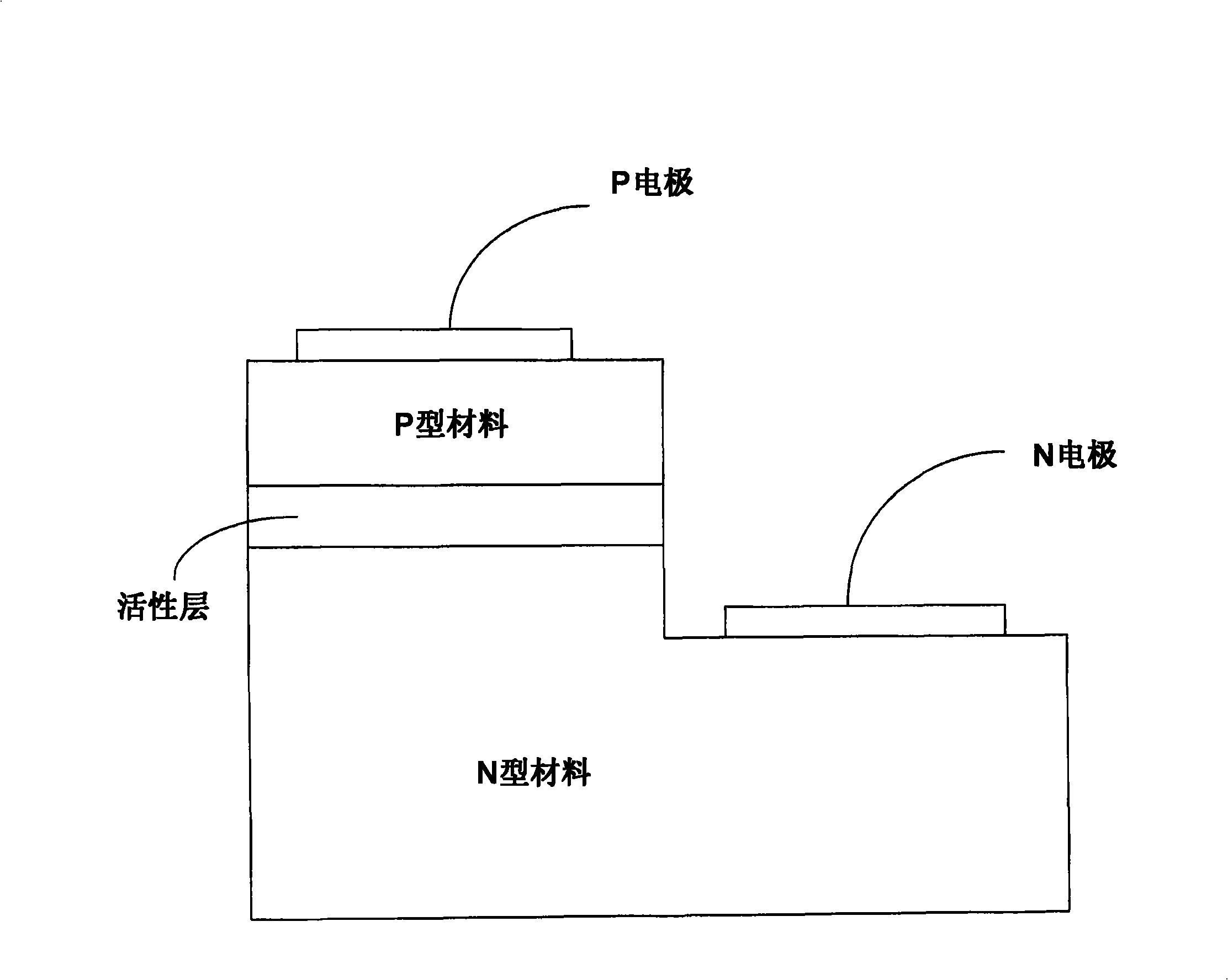
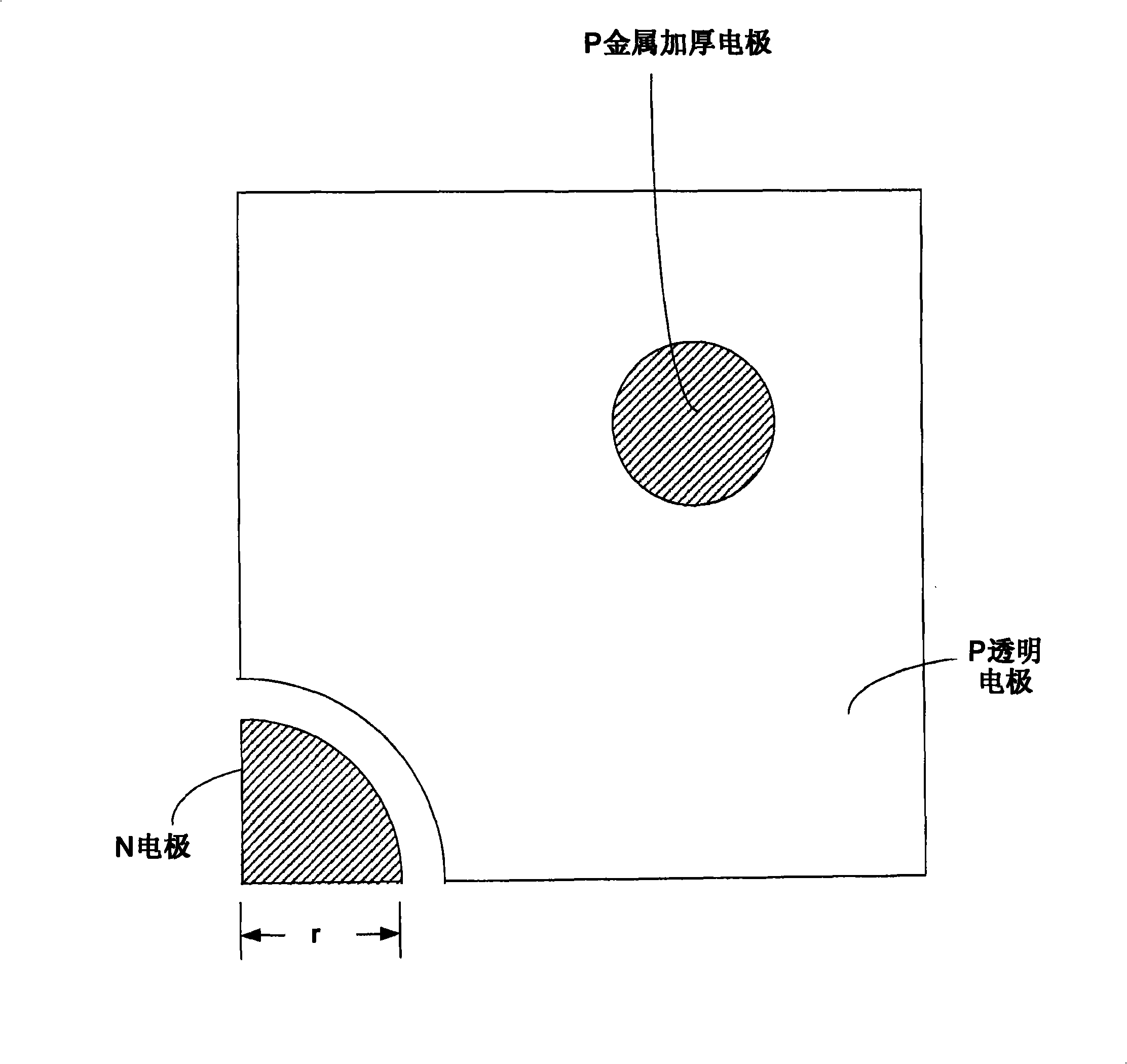
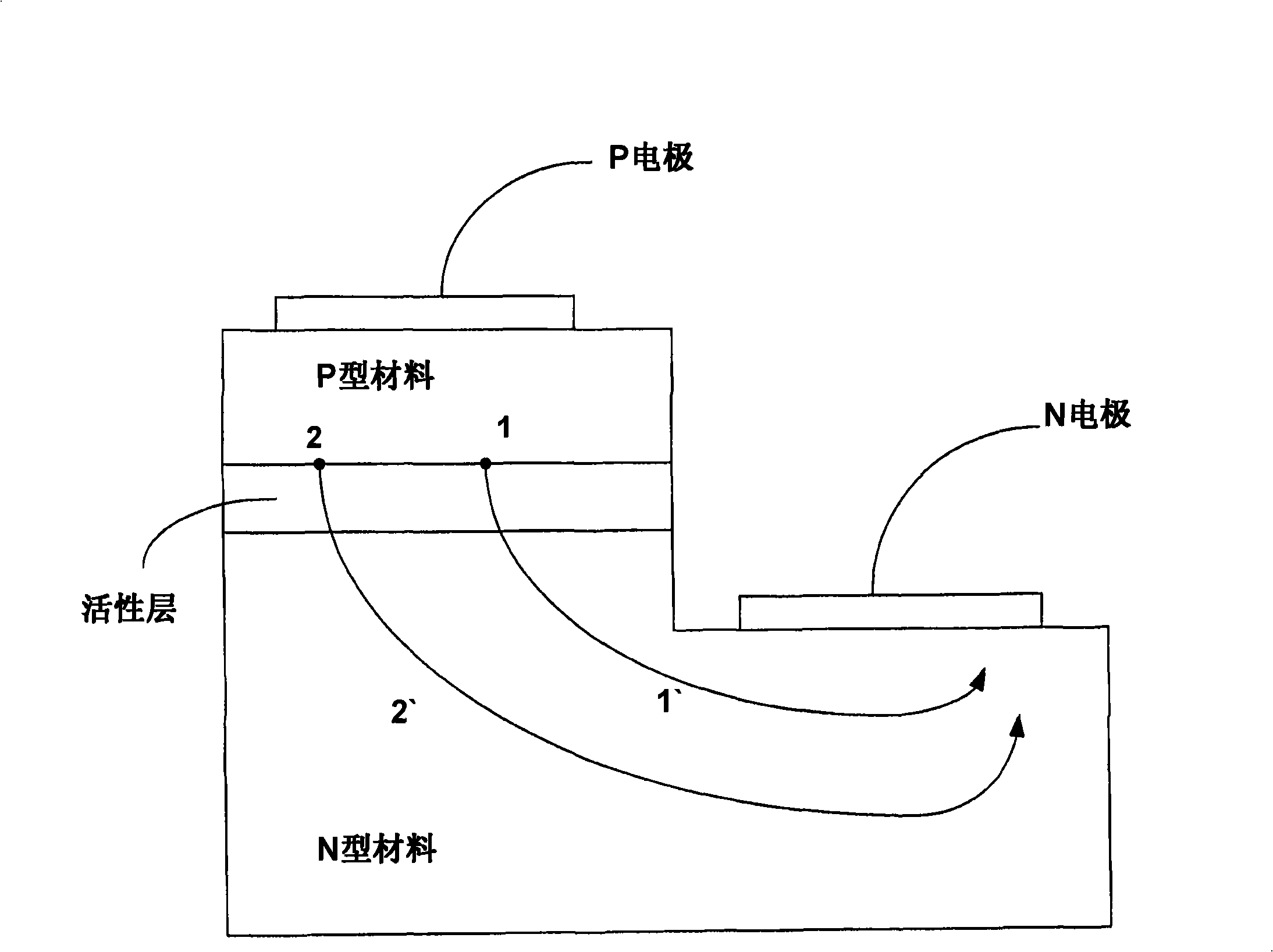
[0027] Figure 4 What is shown is a top view of an LED chip structure according to the present invention. Such as Figure 4 As shown, the LED chip includes a P electrode and an N electrode, wherein the N electrode is located (or approximately located) at the geometric center of the chip, and the P electrode includes a transparent electrode and a thickened electrode, wherein the transparent electrode is located around the N electrode. As mentioned earlier, when the LED is working, the current flowing into the P electrode tends to choose the conduction path with the least resistance to reach the N electrode. Therefore, it is better to enter the N-type material layer from the boundary of the "hollow" ring in the transparent electrode. , and the effect of entering the N-type material at a distance from the boundary of the central ring is secondary. Therefore, it can be considered that the luminous effect of LEDs in a certain place is negatively correlated with the "distance to t...


PUM


Abstract

The invention introduces an LED chip which improves the light-emitting rate and a technique for preparing the LED chip. The LED chip is provided with a first semiconductor material layer in the first conducting type, an active luminescent layer, a second semiconductor material layer with the second conducting type, and an LED chip which is formed from a first and a second electrodes and is arranged on the first and the second semiconductor material layers, wherein the second electrode is composed of a transparent electrode and a first thickening electrode which is positioned in part of the transparent electrode, and the first electrode is positioned on the nongeometric edge of the LED chip and is encircled by the transparent electrode.

Description

technical field [0001] The invention relates to LED chips, in particular to an LED chip design capable of improving light extraction efficiency. Background technique [0002] As a new type of light-emitting device, LED has a wide range of applications in many fields of production and life. LED, the full name of light emitting diode (light emitting diode), usually includes N-type and P-type semiconductor materials, and an active light-emitting layer sandwiched between them, usually a multi-quantum well MQW layer. Normally, electrons and holes are injected into the active light-emitting layer by applying a voltage across the PN junction of the LED. If the electrons and holes undergo radiative recombination, photons will be generated, that is, light of a certain wavelength will be emitted. The color (wavelength) of the emitted light is mainly determined by the forbidden band width of the active light-emitting layer material and the width of the quantum well. [0003] figure ...

Claims


Application Information

Patent Timeline
Patent Type & Authority Applications(China)
IPC IPC(8): H01L33/00
Inventor 郝茂盛邵春林
Owner YUTI LIGHTING SHANGHAI
Why Eureka
Try Eureka