Circuit for preventing gating clock bur
A technology of gated clock and glitch, applied in electrical components, pulse processing, pulse technology, etc., can solve the problems of device failure packaging, chip reliability decline, electrical parameter drift, etc.
- Summary
- Abstract
- Description
- Claims
- Application Information
AI Technical Summary
Problems solved by technology
Method used
Image
Examples
Embodiment Construction
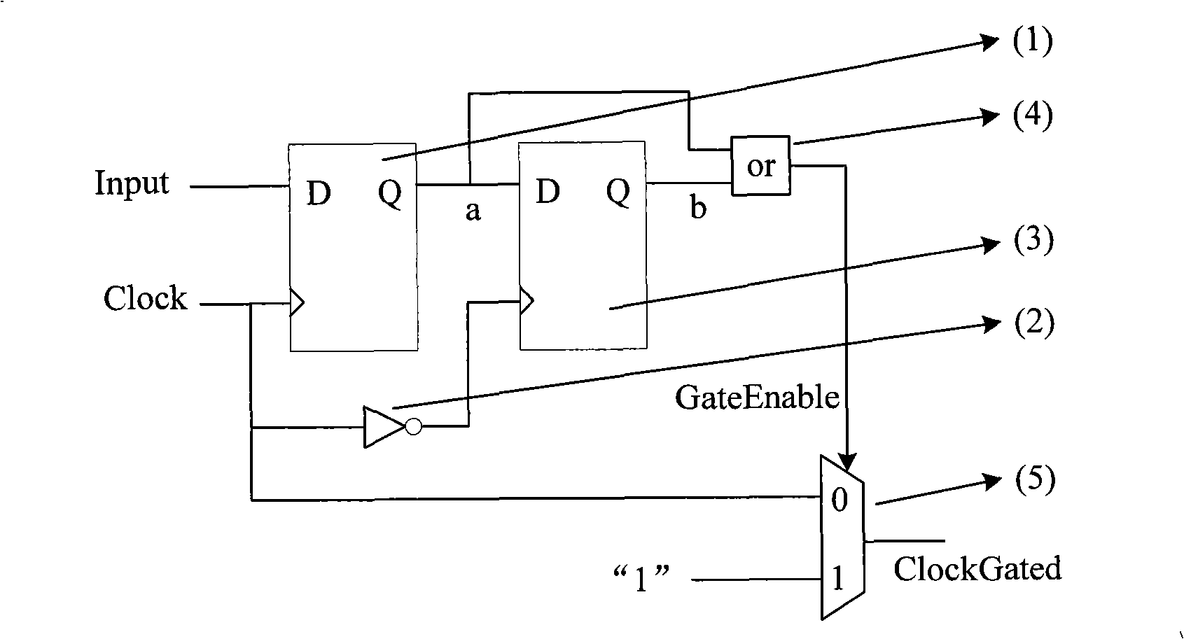
[0017] image 3 It is a circuit structure diagram of the present invention. The main purpose of the circuit of the present invention is to generate a gated clock signal that does not generate glitches.
[0018] At the same time, if two or more input signals of a combinational logic gate change state at the same time, since these input signals are generated through different paths, there is a slight time difference in the moment of their state change, which means This difference may cause some brief intermediate states on the output result signal, forming glitches. These glitches may produce some undesired results and propagate back through the circuit, causing errors in the functionality of the entire circuit. The present invention eliminates the competition between the two input signals of the gating enable signal and the input original clock by designing the timing sequence of the gating enable signal, and avoids inversion in two directions at the same moment, regardless o...
PUM
 Abstract
Description
Claims
Application Information


