Imaging device

A technology of imaging devices and imaging elements, which is applied in installation, image communication, instruments, etc., can solve problems such as adhesive overflow, narrow area, and obstruction of subject imaging, and achieve the effect of preventing bad situations and high gap precision

Active Publication Date: 2009-02-04
KONICA MINOLTA INC
View PDF1 Cites 7 Cited by
  • Summary
  • Abstract
  • Description
  • Claims
  • Application Information

AI Technical Summary

Problems solved by technology

[0007] However, in the case of the above-mentioned Patent Document 1, with the recent thinning of imaging devices, when an infrared absorbing filter formed in the form of a film, that is, an infrared absorbing film (infrared cut member) is attached to a predetermined position with an adhesive, Since the area where the adhesive is applied on the side of the film is narrow, the adhesive may overflow from the side of the film and flow to the surface side
[0008] If the adhesive adheres to the optical path of the object light on the surface of the infrared-absorbing film, it will hinder the imaging of the object, so there is a problem that the imaging device will become a defective product, which is not desirable.

Method used


Image

  • Imaging device
  • Imaging device
  • Imaging device

Examples


Embodiment 1

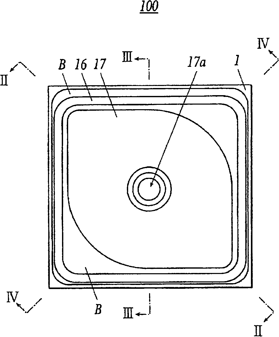
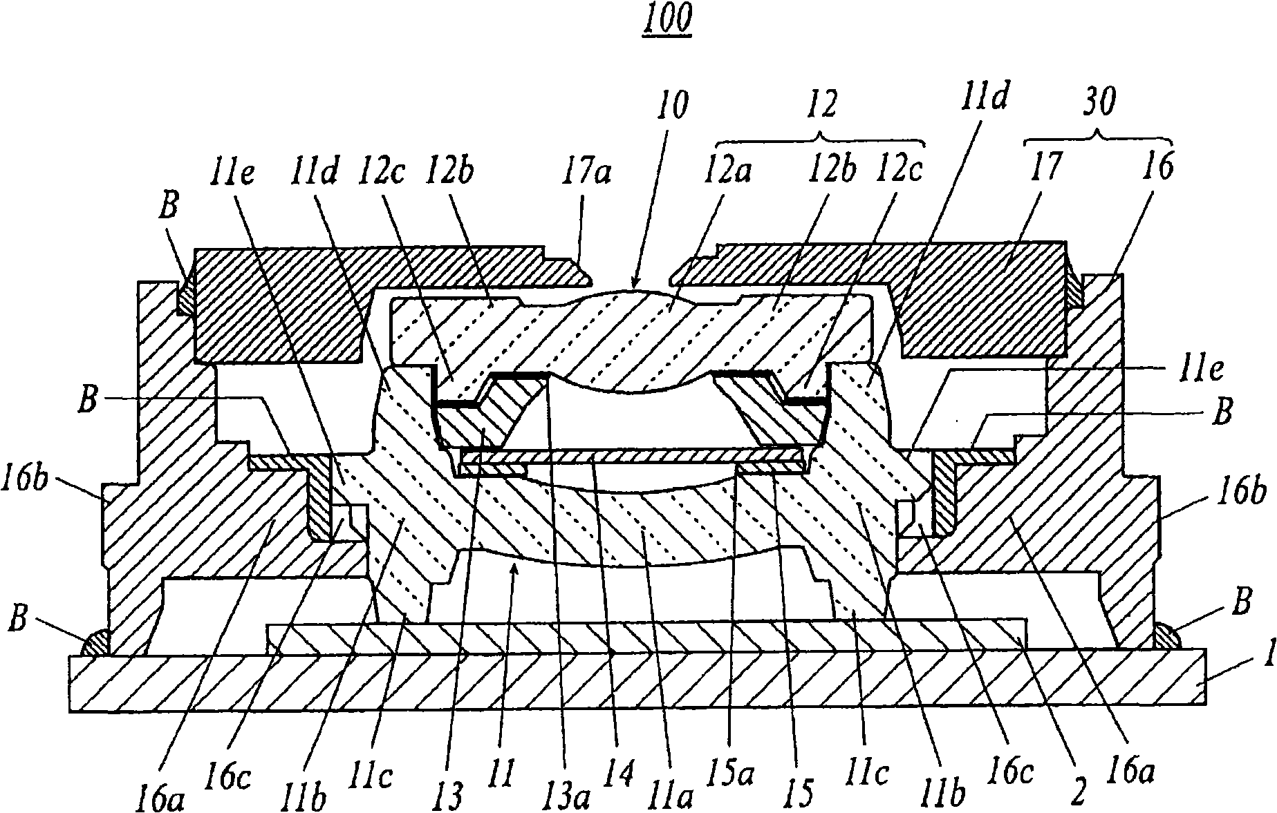
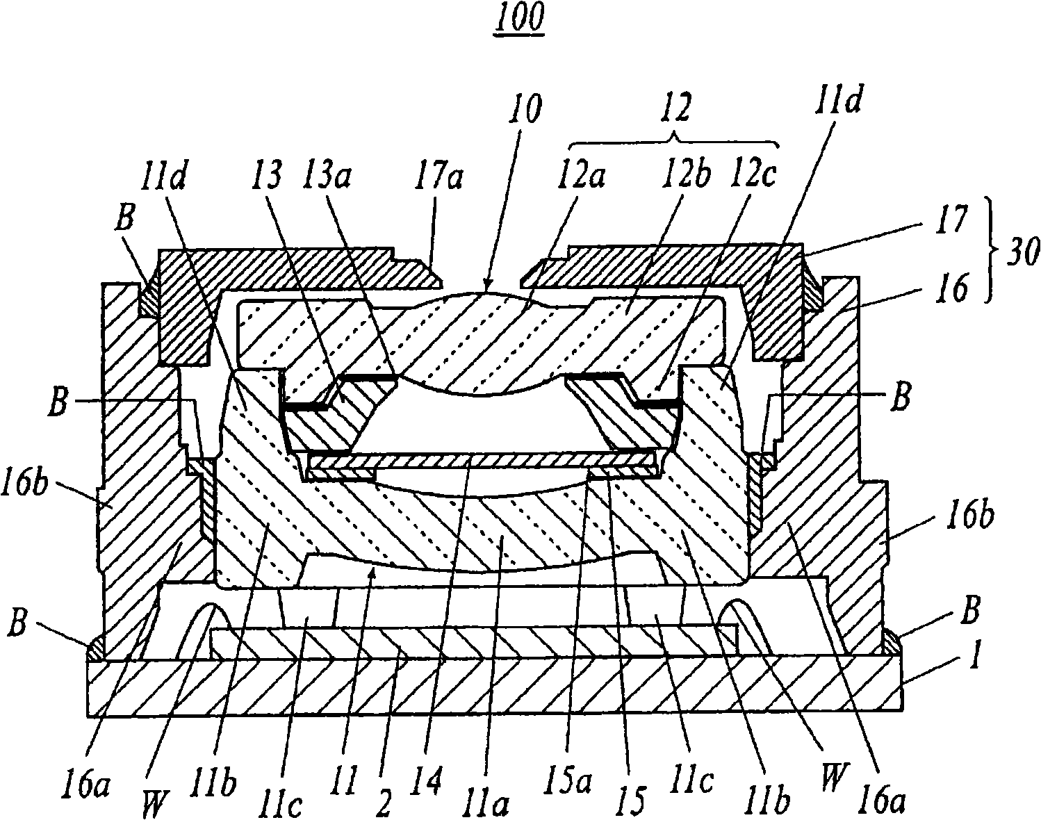
[0042] figure 1 is a plan view of the imaging device 100 of this embodiment, figure 2 yes figure 1 The profile of the II-II line, image 3 yes figure 1 Sectional view of line III-III, Figure 4 yes figure 1 Sectional view of line IV-IV. Figure 5 It is a plan view showing the state where the diaphragm cover 17 of the imaging device 100 is removed.

[0043] Figure 2 ~ Figure 4 In the following description, the front-rear direction along the optical axis direction of the imaging device of the present invention is defined as the up-down direction corresponding to the drawings.

[0044] Such as Figure 1 to Figure 5 As shown, the imaging device 100 includes: a substrate 1, an imaging element 2 disposed on one surface of the substrate 1, an optical assembly 10 disposed on the imaging element 2, an outer frame member 30 covering and hiding the optical assembly 10 and the imaging element 2, etc. .

[0045] The optical assembly 10 includes: a lower lens 11 as an optical comp...


PUM


Abstract

Provided is an imaging device (100). An infrared absorbing film (14) in an imaging device (100) is fixed by being sandwiched between a lower lens (11) and a diaphragm plate (13) which constitute the imaging device (100). Thus, the infrared absorbing film (14) is easily and suitably assembled in the imaging device (100) without using an adhesive.

Description

technical field [0001] The present invention relates to an imaging device, and in particular to an imaging device that can be mounted on electronic equipment such as a mobile phone or a personal computer. Background technique [0002] In recent years, by mounting a small camera device on a small portable terminal (electronic device) such as a mobile phone or a laptop computer, it is possible to transmit not only audio information or text information but also image information over a long distance. [0003] In this imaging device, as an imaging element for imaging a subject and obtaining image data of the subject, a CCD (Charge Coupled Device: Charge Coupled Device) type image sensor or a CMOS (Complementary Metal Oxide Semiconductor: Complementary Metal Oxide Semiconductor) type image sensor, etc. [0004] In addition, the imaging device has an infrared absorption filter that cuts off infrared rays so that they do not reach the imaging element. [0005] An imaging device e...

Claims


Application Information

Patent Timeline
Patent Type & Authority Applications(China)
IPC IPC(8): H04N5/225H04N5/335
CPCH04N5/2254G02B7/022G02B5/208G02B13/0055H04N5/2257G02B7/006H04N23/57H04N23/55
Inventor 上坂武史立林圭介
Owner KONICA MINOLTA INC
Why Eureka
Try Eureka