Polishing apparatus, substrate manufacturing method, and electronic apparatus manufacturing method

A technology for polishing devices and substrates, which is applied in the direction of grinding/polishing safety devices, surface polishing machine tools, manufacturing tools, etc., and can solve the problems of not considering the prevention and removal of dust, and the inability to provide high-quality polishing processes, etc.

Inactive Publication Date: 2009-02-11
FUJITSU LTD
View PDF3 Cites 21 Cited by
  • Summary
  • Abstract
  • Description
  • Claims
  • Application Information

AI Technical Summary

Problems solved by technology

The double-side polishing device described in JP 1-92063 does not consider dust prevention and removal, and the double-side polishing device cannot provide a high-quality polishing process

Method used


Image

  • Polishing apparatus, substrate manufacturing method, and electronic apparatus manufacturing method
  • Polishing apparatus, substrate manufacturing method, and electronic apparatus manufacturing method
  • Polishing apparatus, substrate manufacturing method, and electronic apparatus manufacturing method

Examples


Embodiment Construction

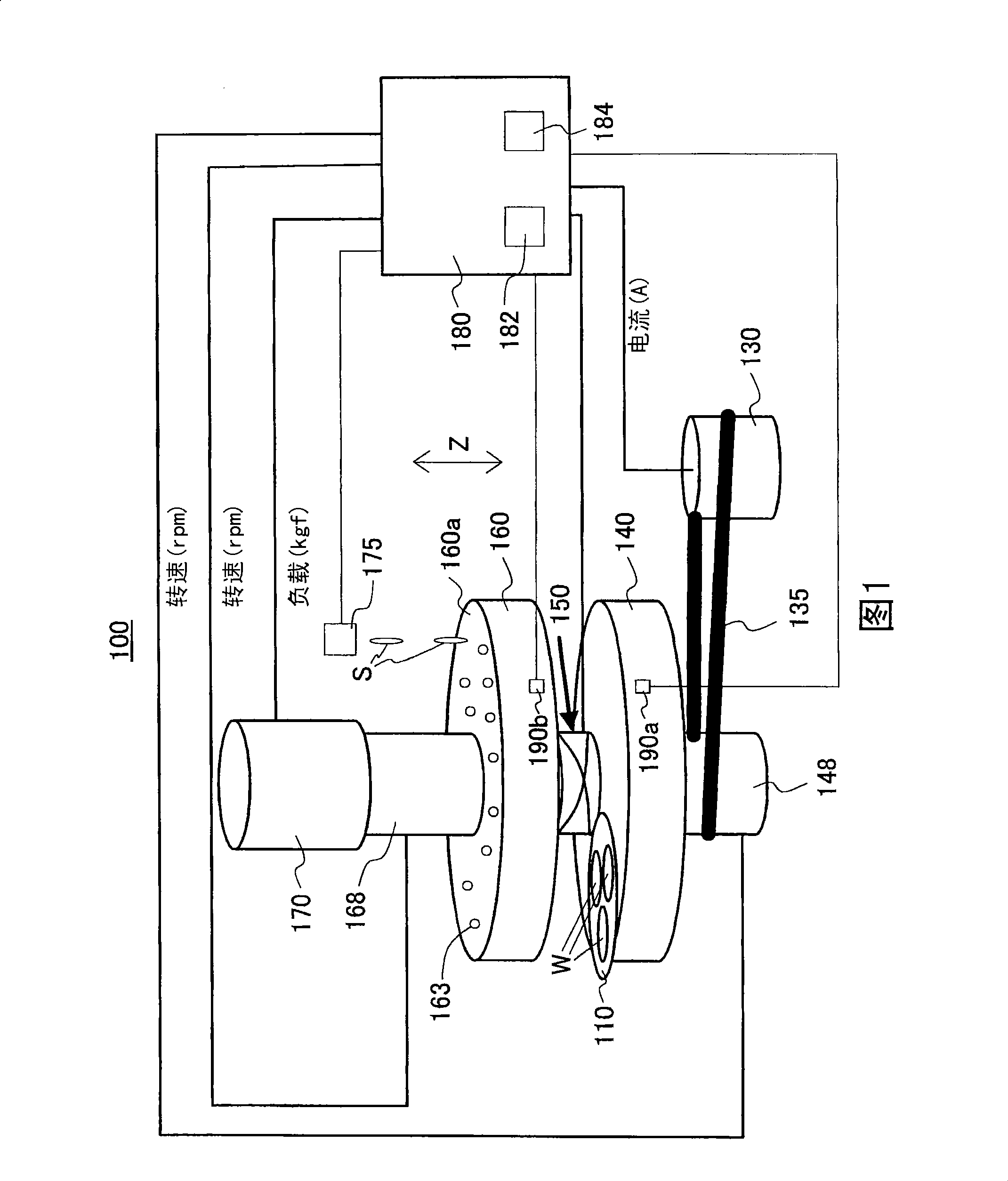
[0052] Referring now to the drawings, a polishing apparatus 100 according to an embodiment of the present invention will be described. FIG. 1 is a schematic perspective view of a polishing apparatus 100 according to the present invention. The polishing apparatus 100 is configured to simultaneously polish both surfaces of the workpiece W by chemical mechanical polishing, however, the polishing apparatus of the present invention is applicable to any polishing apparatus other than a CMP apparatus such as a polishing apparatus for finishing.

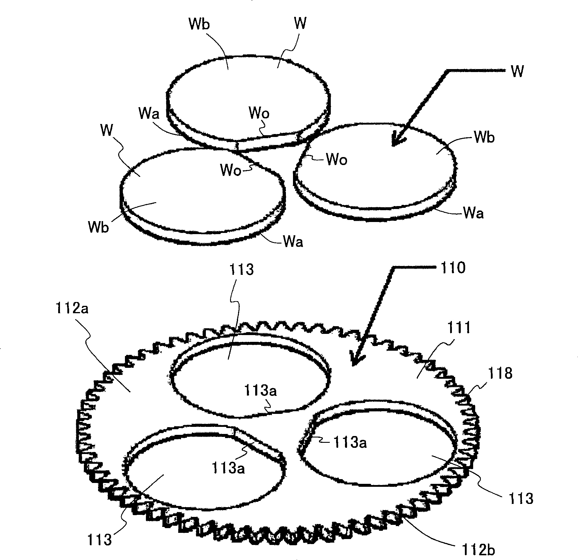
[0053] The workpiece W of this embodiment is a substrate, which is a target to be polished. Substrates include glass substrates, silicon substrates, ceramic substrates (including laminate substrates), and any other substrate made of single crystal material. Typical shapes of these substrates are disks (in the case of wafers, disks with an orientation flat) or rectangular plates. Usually, the diameter or length of the substrate is about ten...


PUM


Abstract

The invention discloses a polishing apparatus, substrate manufacturing method, and electronic apparatus manufacturing method. The polishing apparatus is configured to simultaneously polish both surfaces of a work and includes a sun gear provided around a rotational axis of one of a pair of polishing surfaces, a carrier having a hole configured to house the work, and including teeth so as to serve as a planetary gear which rotates and revolves around the sun gear, and a first dustproof mechanism that includes a first elastic member that contacts one surface of the carrier opposite to one of the polishing surfaces between the sun gear and the hole in the carrier.

Description

[0001] This application claims foreign priority based on Japanese Patent Application No. 2007-208397 filed on August 9, 2007, the entire contents of which are incorporated herein by reference. technical field [0002] The present invention relates generally to a polishing apparatus, and more particularly to an apparatus for polishing both surfaces of a workpiece. For example, the present invention can be applied to a chemical mechanical polishing device or a chemical mechanical planarization polishing device (abbreviated as: CMP device). Background technique [0003] A micro-electro-mechanical system (abbreviation: MEMS) sensor is an example of MEMS, which needs to be kept in a vacuum environment by bonding a glass substrate to both sides of a MEMS chip having a sensing function. Therefore, the MEMS chip side of the glass substrate needs to have high flatness. The manufacturing process will be more convenient if there is no need to distinguish the front and rear surfaces of...

Claims


Application Information

Patent Timeline
Patent Type & Authority Applications(China)
IPC IPC(8): B24B29/00H01L21/00H01L21/304H01L21/3105B24B37/08B24B55/06
CPCB24B55/04B24B37/08H01L21/304
Inventor 十仓史彦竹内光生
Owner FUJITSU LTD
Why Eureka
Try Eureka