Array substrate and defect detecting method thereof

An array substrate and defect detection technology, applied in nonlinear optics, instruments, optics, etc., can solve problems such as unguaranteed production speed, time-consuming, and wrong judgments by manual visual inspection.

Active Publication Date: 2009-02-11
KUSN INFOVISION OPTOELECTRONICS
View PDF0 Cites 59 Cited by
  • Summary
  • Abstract
  • Description
  • Claims
  • Application Information

AI Technical Summary

Problems solved by technology

However, with the continuous increase of the size of the liquid crystal panel, this kind of inspection is more and more difficult to meet the requirements, mainly because: on the one hand, it takes too much time to guarantee the production speed; risk

Method used


Image

  • Array substrate and defect detecting method thereof
  • Array substrate and defect detecting method thereof
  • Array substrate and defect detecting method thereof

Examples


no. 1 example

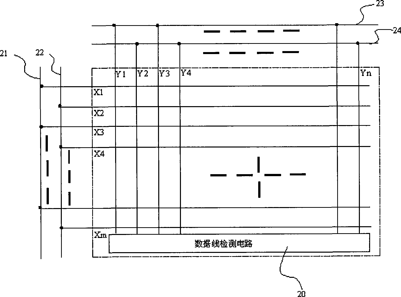
[0028] First refer to Figure 2 to Figure 6B A first embodiment of the present invention will be described. figure 2 is a schematic diagram of an array substrate provided with a data line detection circuit according to a first embodiment of the present invention. The structure of this array substrate and figure 1 Similar to the array substrate, it is also an array substrate with m rows and n columns. On the periphery of the array substrate (that is, the blank area of ​​the non-array substrate on the mother glass substrate), there are: electrically connected odd-numbered row gate lines (X1 , X3...Xm-1) the first grid short-circuit bar 21, electrically connected to the second grid short-circuit bar 22 of the even-numbered row gate lines (X2, X4...Xm); and electrically connected to the odd-numbered column data lines (Y1 , Y3 ... Yn-1) the first data short bar 23 is electrically connected to the second data short bar 24 of the even column data lines (Y2, Y4 ... Yn). The array ...

no. 2 example

[0041] The above description is aimed at the array substrate and the method thereof for detecting and locating the line defects of the data lines. For the gate lines, a similar gate line detection circuit can also be used for processing. refer to Figure 7 , Figure 7 It is a schematic diagram of an array substrate provided with a gate line detection circuit 70 according to a second embodiment of the present invention. Such as Figure 7 As shown, the gate line detection circuit 70 is disposed in the non-display area on the right side of the array substrate. Figure 7 The gate line detection circuit 70 shown can receive the voltage signal transmitted by the gate line, so as to detect and locate the line defect of the gate line. The gate line detection circuit 70 may have the same configuration as the data line detection circuit in the first embodiment except that m gate lines are connected. In addition, the gate line detection method performed by the gate line detection ci...

no. 3 example

[0043] In addition to providing only one data line detection circuit or one gate line detection circuit, a data line detection circuit and a gate line detection circuit may also be provided at the same time to detect defects of the data line and the gate line. Figure 8is a schematic diagram of an array substrate provided with a data line detection circuit and a gate line detection circuit according to a third embodiment of the present invention. Such as Figure 8 As shown, the data line detection circuit 80 and the gate line detection circuit 90 are respectively disposed in the non-display area below and right of the array substrate. Figure 8 The data line detection circuit 80 shown can receive the voltage signal transmitted by the data line, so as to detect and locate the line defect of the data line. The gate line detection circuit 90 can receive the voltage signal transmitted by the gate line, so as to detect and locate the line defect of the gate line. The data line de...


PUM


Abstract

The invention discloses an array basal plate and a method for detecting the defects thereof. The array basal plate includes one or more shorting bars used for applying signals on a plurality of data lines and a plurality of grid lines of the array basal plate during the detection. The array basal plate is characterized in that the array basal plate further includes a line detection circuit used for receiving the signals on the data lines and the grid lines, and detecting and positioning the defects of the data lines and the grid lines. The array basal plate and the method for detecting the defects thereof can accurately and rapidly position the line defects on the array basal plate.

Description

technical field [0001] The invention relates to an array substrate and a defect detection method thereof. Background technique [0002] Liquid crystal displays are widely used due to their advantages of lightness, thinness, portability and environmental protection. Generally speaking, a liquid crystal display includes an array substrate and a color filter substrate disposed opposite to each other, and a liquid crystal layer sandwiched between the two substrates. A plurality of gate lines and a plurality of data lines are arranged on the array substrate, and the plurality of gate lines and the plurality of data lines are vertically intersected to define a plurality of pixel areas. Thin film transistors (TFTs). In the production process, a large number of gate lines and data lines will cause line defects (hereinafter referred to as "line defects") due to some production defects, such as short circuit, open circuit, etc., thereby forming display defects of the liquid crystal ...

Claims


Application Information

Patent Timeline
Patent Type & Authority Applications(China)
IPC IPC(8): G02F1/1362G02F1/13G09G3/36
CPCG09G3/006G02F1/1309G09G2330/12
Inventor 钟德镇简廷宪邱郁雯廖家德
Owner KUSN INFOVISION OPTOELECTRONICS
Why Eureka
Try Eureka