Image sensing device

An image sensing element and image sensor technology, applied in electrical elements, electrical solid-state devices, semiconductor devices, etc., can solve problems such as propagation loss, and achieve the effect of isolating light, reducing light, and avoiding diffraction and crosstalk.

Inactive Publication Date: 2009-02-11
MEDIATEK INC
View PDF0 Cites 14 Cited by
  • Summary
  • Abstract
  • Description
  • Claims
  • Application Information

AI Technical Summary

Problems solved by technology

[0003] However, traditional fingerprint sensors suffer from issues such as crosstalk, loss propagation, and diffraction

Method used


Image

  • Image sensing device
  • Image sensing device
  • Image sensing device

Examples


Embodiment Construction

[0016] In order to make the above-mentioned and other objects, features, and advantages of the present invention more obvious and understandable, the preferred embodiments are specifically listed below, together with the accompanying drawings in the description, and are described in detail as follows:

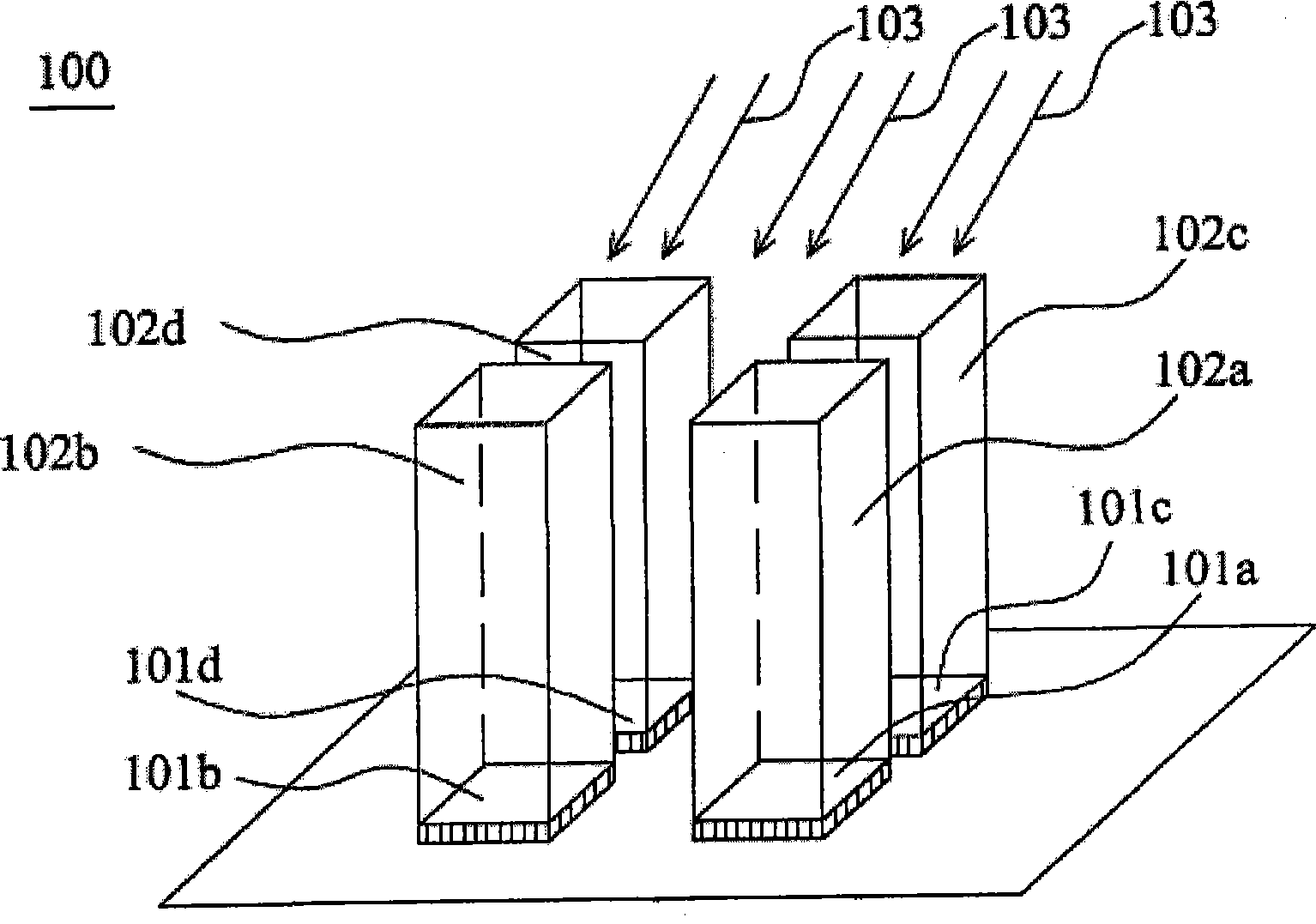
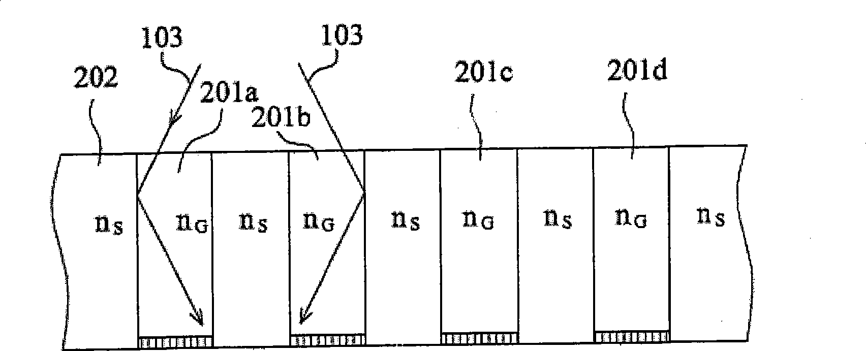
[0017] figure 1 is a schematic diagram showing the structure of an image sensing device according to an embodiment of the present invention. Such as figure 1 As shown, the image sensing device 100 includes image sensor units 101a, 101b, 101c, 101d and waveguide units 102a, 102b, 102c, 102d. The image sensor units 101a, 101b, 101c, 101d are independently disposed on a surface with a predetermined distance between them. The incident light 103 is guided by the waveguide units 102 a , 102 b , 102 c , and 102 d to enter the image sensor units 101 a , 101 b , 101 c , and 101 d respectively. In this embodiment, the refractive index of the waveguide units 102a, 102b, 102c, 102d is g...


PUM


Abstract

An image sensing device is disclosed. The image sensing device comprises a plurality of image sensor units disposed separately and a plurality of wave guiding units. Each wave guiding unit is disposed on each corresponding image sensor unit. The image sensing device can avoid diffraction and crosstalk. In addition, since each interlayer distance is short, the effect to isolate beams and reduce propagation loss is reached to some degree.

Description

technical field [0001] The invention relates to an electronic device, and in particular to an image sensing device. Background technique [0002] Fingerprint sensing and matching is a reliable and widely used technology for personal identification and verification. In particular, there is a common fingerprint identification method that includes scanning a fingerprint sample and / or image and storing the unique features of the image and / or fingerprint image. The characteristics of the fingerprint sample will be compared with the fingerprint data already stored in the database to identify and confirm the identity of the individual. [0003] However, conventional fingerprint sensors suffer from issues such as crosstalk, loss propagation, and diffraction. Therefore, the industry urgently needs an image sensing device (eg, a fingerprint sensor) that can solve the above problems. Contents of the invention [0004] In order to overcome the unavoidable technical problems of cros...

Claims


Application Information

Patent Timeline
Patent Type & Authority Applications(China)
IPC IPC(8): G06K9/00
CPCG06K9/00046H01L27/14625G06V40/1324
Inventor 汪盈宗洪浩评杨瑞青
Owner MEDIATEK INC
Why Eureka
Try Eureka