
Sheet peeling device and sheet printing system using same device

A technology of stripping device and printing system, which is applied in the direction of assembling printed circuit, printed circuit, and printed circuit manufacturing of electrical components, which can solve problems such as poor contact and achieve the effect of preventing poor insulation

Inactive Publication Date: 2009-03-11
HITACHI LTD
View PDF1 Cites 3 Cited by
  • Summary
  • Abstract
  • Description
  • Claims
  • Application Information

AI Technical Summary

Problems solved by technology

In addition, after reflowing, the sheet must be peeled off from the circuit board, so the residue of the sheet may remain on the substrate, causing poor contact, etc., and the sheet must be removed without leaving residue

Method used


Image

  • Sheet peeling device and sheet printing system using same device
  • Sheet peeling device and sheet printing system using same device
  • Sheet peeling device and sheet printing system using same device

Examples


Embodiment Construction

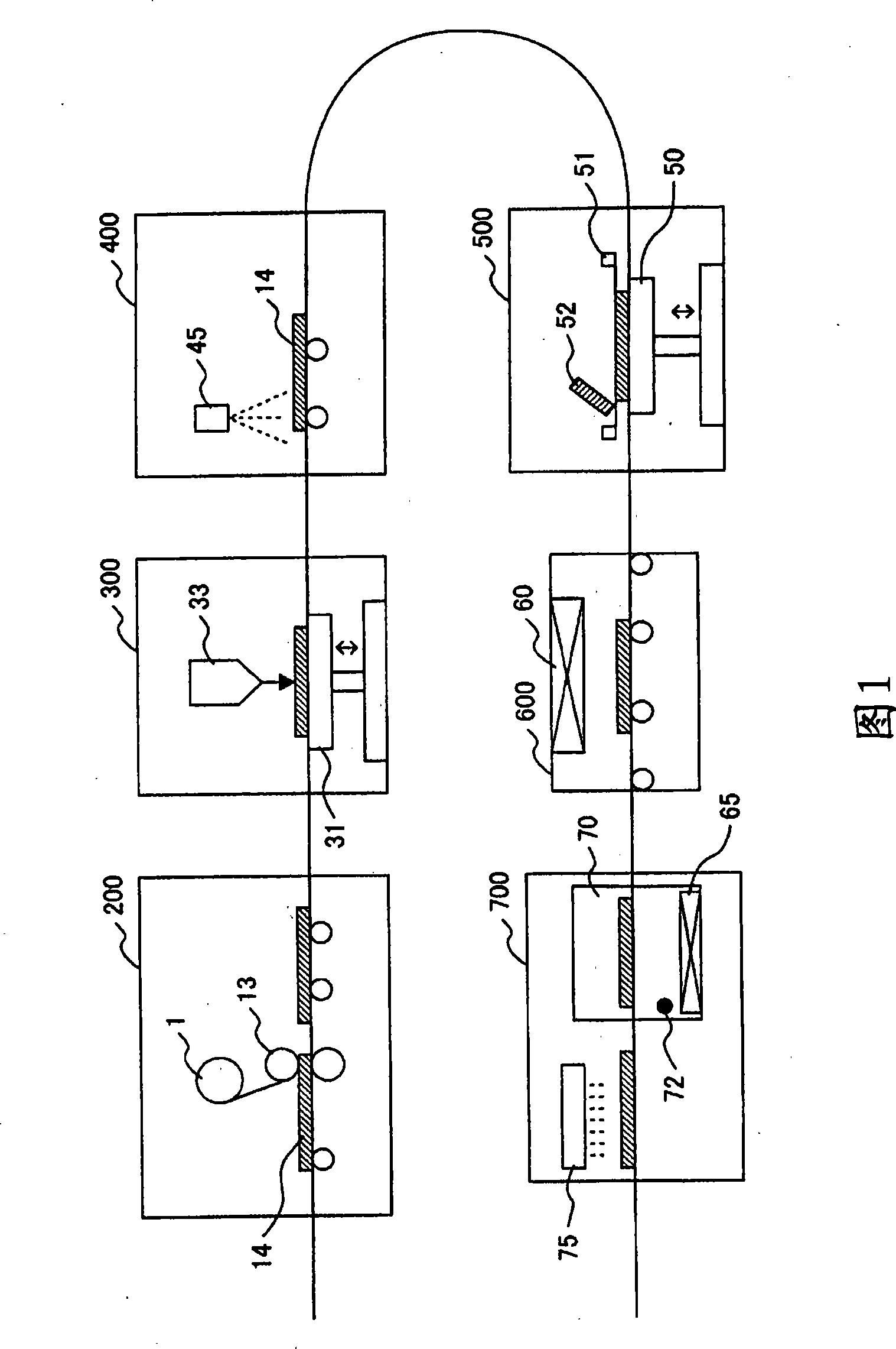
[0014] FIG. 1 schematically shows the overall structure of a sheet printing system.

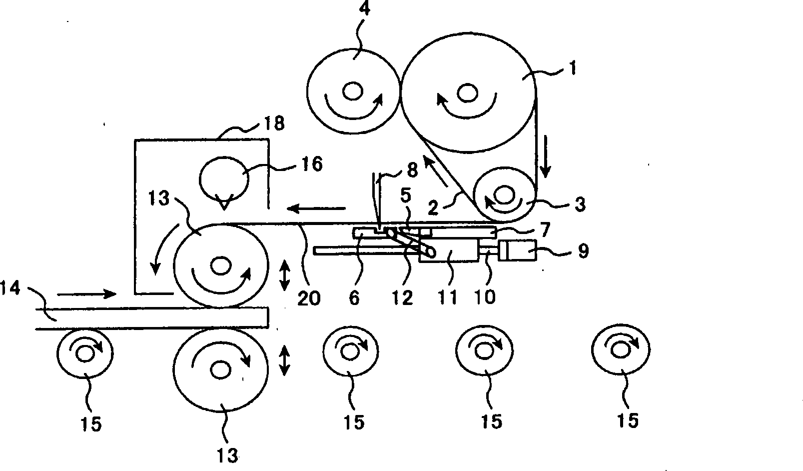
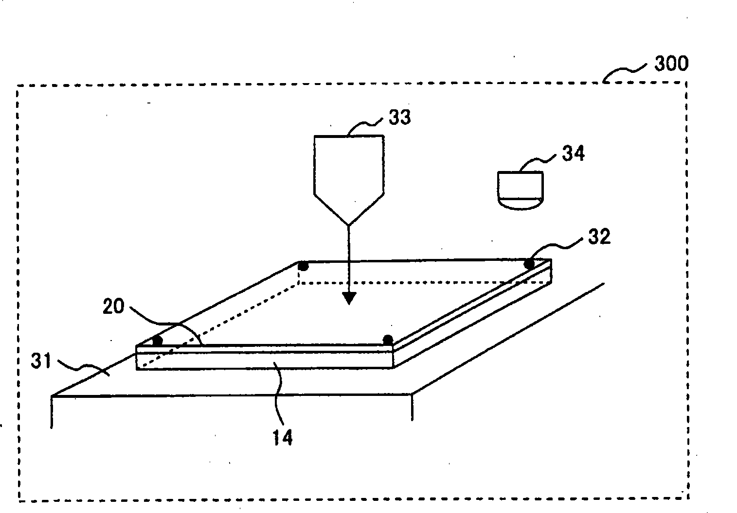
[0015] As shown in the figure, this system includes a film sticking device 200 , a pattern making device 300 , a cleaning device 400 , a printing device 500 , a reflow device (reflow oven) 600 , and a film peeling device 700 . The above-mentioned film sticking device 200 sticks the sheet-like member 20 (or sometimes referred to as a film) to the printing surface of the substrate 14 which is the printing target. The above-mentioned pattern making apparatus 300 performs perforation processing of a pattern printed by a laser or an exposure method on the surface of the pasted sheet. The cleaning device 400 described above removes residues on the surface of the sheet material subjected to the perforation process. The above-mentioned printing device 500 is equipped with a mask, and an opening approximately the same as or slightly smaller than that of the substrate surface is provided on the mask, ...


PUM


Abstract

The invention claims a sheet printing system, in which undesirable printing caused by dislocation of a sheet component will not be brought when arranging an opening on the sheet component and printing by supplying soldering paste to the opening, comprising a paste portion, a pattern making portion, a printing portion, a backflow furnace and a stripping portion, characterized in that the paste portion pastes the sheet component onto a base plate for coating soldering paste; the pattern making portion forms an opening pattern for coating soldering paste on the sheet component; the printing portion prints soldering paste on the base plate mounting with the sheet component that forms the opening pattern; the backflow furnace heats the base plate printing with soldering paste to fix the soldering paste onto surface of the base plate; and the stripping portion removes the sheet component from the surface of the base plate fixing with soldering paste.

Description

technical field [0001] The present invention relates to a printing device for forming solder bumps on a substrate, in particular to a printing system for printing with a sheet-like component as a mask. Background technique [0002] Japanese Patent Application Laid-Open No. 9-116257 discloses a technique for forming solder bumps in a desired pattern on a substrate surface. In this technique, a pattern is formed on a sheet member, a masking sheet having the same pattern as the pattern formed on the sheet is placed, and solder paste is filled on the sheet member from the top of the masking sheet, and then removed. After the mask sheet is prepared, the sheet-shaped component filled with solder paste is placed on the substrate so that it is aligned with the substrate surface, and after reflowing, the sheet is removed to form a desired pattern on the substrate surface. Brazing bumps. [0003] In the above technique, it is necessary to use a masking sheet having the same pattern ...

Claims


Application Information

Patent Timeline
Patent Type & Authority Applications(China)
IPC IPC(8): H05K3/34
CPCH05K3/04H05K13/0465H05K13/0486H05K2203/0139H05K2203/043
Inventor 川边伸一郎向井范昭五十岚章雄和田正文
Owner HITACHI LTD
Learn More