Scanning optical apparatus
a scanning optical apparatus and optical apparatus technology, applied in the field of scanning optical apparatus and multi-beam scanning optical apparatus, can solve the problems of difficult construction of compact scanning optical apparatus, long distance from the f lens to the surface to the scanned, and the thickness of the f lens, so as to achieve high-quality printing.
- Summary
- Abstract
- Description
- Claims
- Application Information
AI Technical Summary
Benefits of technology
Problems solved by technology
Method used
Image
Examples
embodiment 1
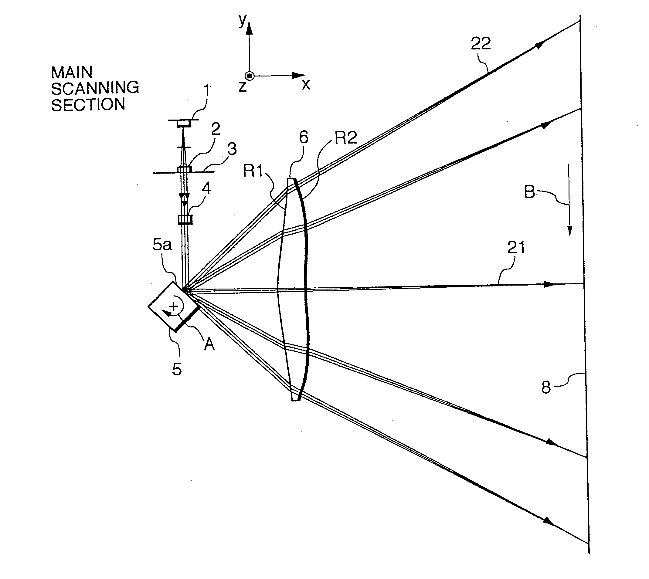
[0097]FIGS. 4A and 4B are cross-sectional views of Embodiment 1 of the present invention in the main scanning direction and the sub scanning direction, respectively.
[0098]In these figures, reference numeral 1 designates light source means (a light source unit) comprising, for example, a semiconductor laser.
[0099]Reference numeral 2 denotes a collimator lens as a first optical element which converts a divergent beam of light emitted from the light source means 1 into a convergent beam of light. Reference numeral 3 designates an aperture stop which regularizes the diameter of the beam of light passing therethrough.
[0100]Reference numeral 4 denotes a cylindrical lens as a second optical element which has predetermined refractive power only in the sub scanning direction and causes the beam of light passed through the aperture stop 3 to be imaged as a substantially linear image on the deflecting surface 5a of a light deflector (deflecting element) 5 which will be described later in the s...
embodiment 2
[0112]FIGS. 8A and 8B are cross-sectional views of Embodiment 2 of the present invention in the main scanning direction and the sub scanning direction, respectively. In FIGS. 8A and 8B, the same elements as the elements shown in FIGS. 4A and 4B are given the same reference numerals.
[0113]The differences of Embodiment 2 from the aforedescribed Embodiment 1 are that the divergent beam of light emitted from the semiconductor laser (the light source unit) is converted not into a convergent beam of light but into a parallel beam of light by the collimator lens and that corresponding thereto, the lens shape of the fθ lens is made different. In the other points, the construction and optical action of Embodiment 2 are substantially similar to those of Embodiment 1, whereby a similar effect is obtained.
[0114]Table 2 below shows the optical arrangement in Embodiment 2 and the aspherical surface coefficients of an fθ lens 26.
TABLE 2 (Embodiment 2)wavelength usedλ (nm)780refractive index of fθ ...
embodiment 3
[0119]FIGS. 12A and 12B are cross-sectional views of Embodiment 3 of the present invention in the main scanning direction and the sub scanning direction, respectively. In these figures, the same element as the elements shown in FIG. 4 are given the same reference numerals.
[0120]The differences of Embodiment 3 from the aforedescribed Embodiment 1 are that the apparatus is comprised of a multibeam scanning optical system for scanning a plurality of beams of light emitted from light source means 11 having a plurality of (in Embodiment 3, too) light source units capable of being independently modulated, at a time, so as to have a predetermined interval therebetween on the surface to be scanned, and that correspondingly thereto, the lens shape of the fθ lens in the meridian-line direction (the sub scanning direction) is made different. In the other points, the construction and optical action of Embodiment 3 are substantially similar to those of the aforedescribed Embodiment 1, whereby a ...
PUM
 Abstract
Description
Claims
Application Information


