Manufacturing method of LED element

A technology for light-emitting diodes and a manufacturing method, which is applied to electrical components, semiconductor devices, circuits, etc., can solve problems such as difficulty in etching, inability to etch slopes, etc., and achieve the effects of simple fabrication, improved light extraction rate, and reduced production costs.

Inactive Publication Date: 2009-03-18
TEKCORE CO LTD
View PDF2 Cites 36 Cited by
  • Summary
  • Abstract
  • Description
  • Claims
  • Application Information

AI Technical Summary

Problems solved by technology

However, due to the strong bonding between atoms in GaN series light-emitting diodes, it is extremely difficult to etch the bevel angle with lattice orientation characteristics in the GaN epitaxial layer. If only wet etching is used, it cannot be etched. slope out

Method used


Image

  • Manufacturing method of LED element
  • Manufacturing method of LED element
  • Manufacturing method of LED element

Examples


Embodiment Construction

[0017] The detailed content and technical description of the present invention will be further described by examples, but it should be understood that these examples are for illustrative purposes only, and should not be construed as limitations on the implementation of the present invention.

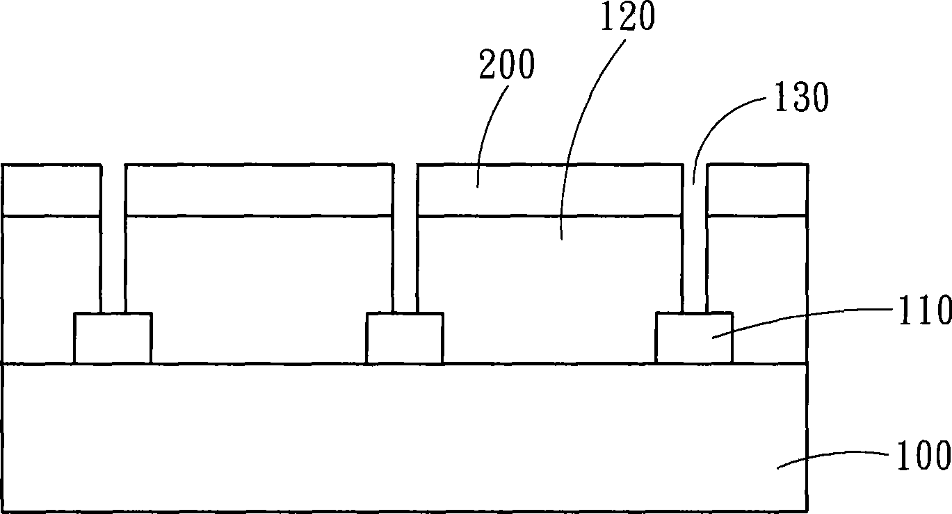
[0018] The invention utilizes the combination of the epitaxial method and the etching method to make the epitaxial layer structure of the light-emitting diode form a non-rectangular slope, improve the phenomenon of total reflection at the interface, and manufacture a light-emitting diode element with a high light extraction rate.

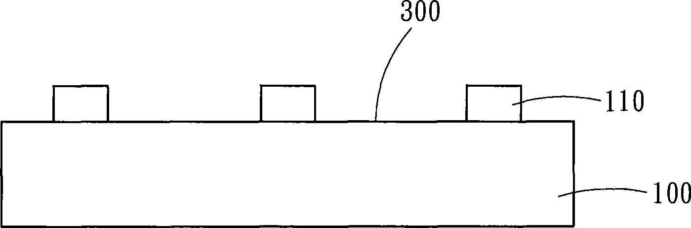
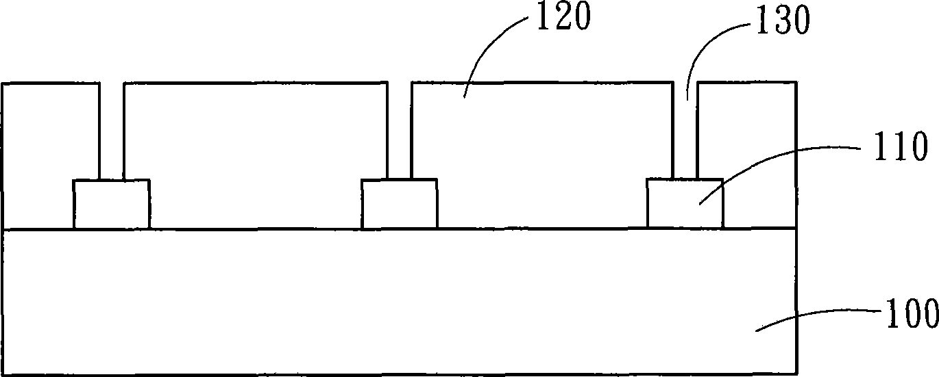
[0019] see Figure 1 to Figure 7 , is a schematic flow chart of the manufacturing method of the first embodiment of the present invention. The manufacturing steps of the first embodiment of the present invention include:

[0020] (a) A substrate 100 is provided, a shielding layer 110 is formed on the surface of the substrate 100, and the shielding layer 110 de...


PUM


Abstract

The invention relates to a production method of a light-emitting diode, which comprises facilitating the epitaxial layer of the light-emitting diode to start etching from the bottom to form a structural shape whose side is overhung and projected through combining the epitaxial way and the etching way, and leading the epitaxial layer of the light-emitting diode to change into a non-rectangular inclined plane, thereby improving the phenomenon of interface total reflection of the light-emitting diode, and increasing the light sending rate of the light-emitting diode. The invention can reduce production cost owing to simple manufacture, and is suitable to be produced in industrialization.

Description

technical field [0001] The invention relates to a method for manufacturing a light-emitting diode element, in particular to a method for manufacturing a light-emitting diode element with a high light extraction rate. Background technique [0002] Traditional light-emitting diode components are made with a standard rectangular appearance, because the refractive index of the general light-emitting diode itself is very different from that of the outside air or packaging materials, making it easy for light to produce total reflection at the interface, so the light-emitting diode When the generated light reaches the interface with the air, the light greater than the critical angle will be totally reflected back to the inside of the diode grain. In addition, the four cross-sections of the rectangle are parallel to each other, and the probability of photons leaving the semiconductor at the interface is reduced, so that the photons can only be totally reflected inside until they are...

Claims


Application Information

Patent Timeline
Patent Type & Authority Applications(China)
IPC IPC(8): H01L33/00H01L33/20
Inventor 许文杰刘育全富振华李适宏王泰钧
Owner TEKCORE CO LTD
Why Eureka
Try Eureka