Stacked 1t-n memory cell structure
A technology of memory cells and memory elements, applied in the field of reading circuits, can solve problems such as not being able to be integrated so densely
- Summary
- Abstract
- Description
- Claims
- Application Information
AI Technical Summary
Problems solved by technology
Method used
Image

Examples
Embodiment Construction
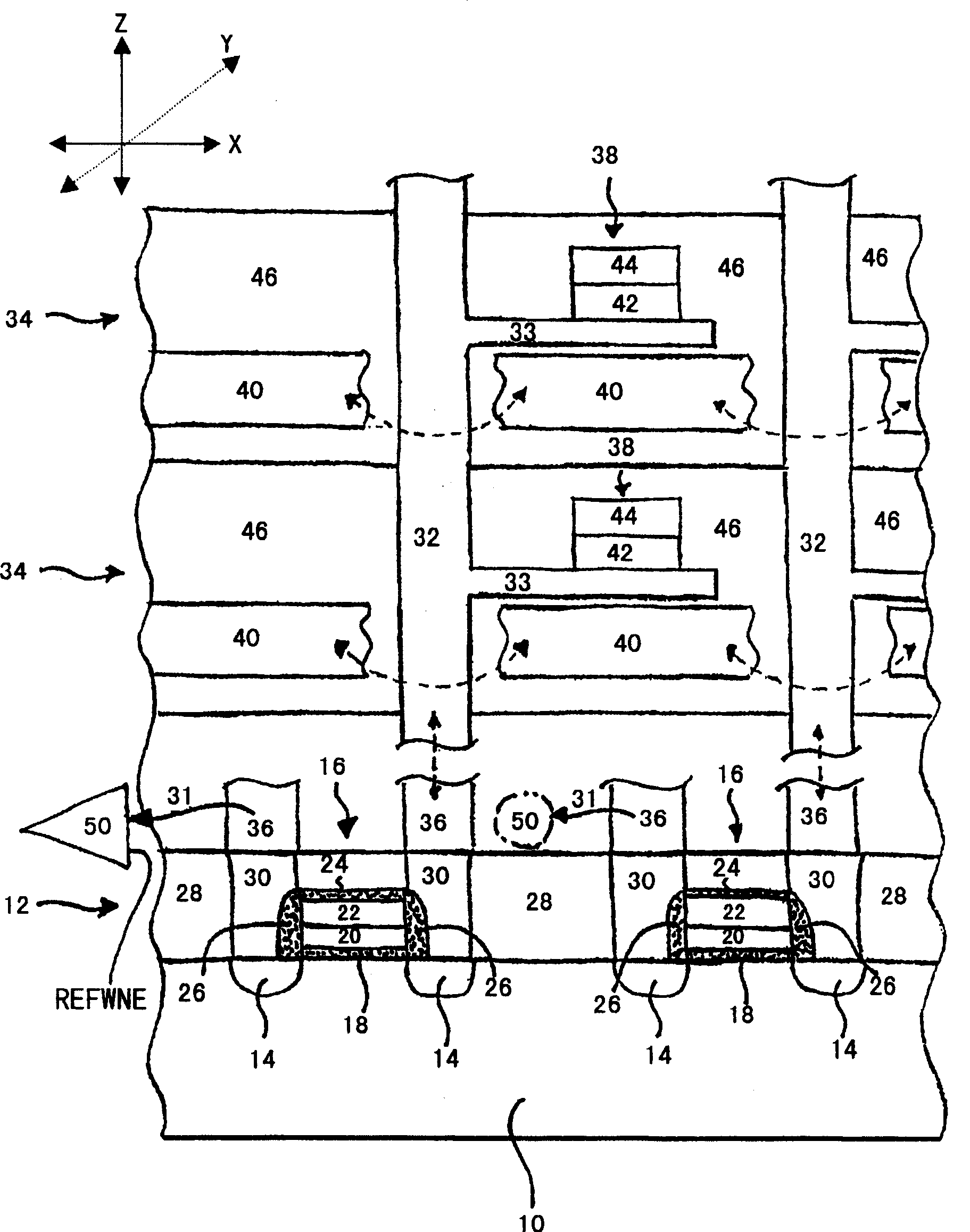
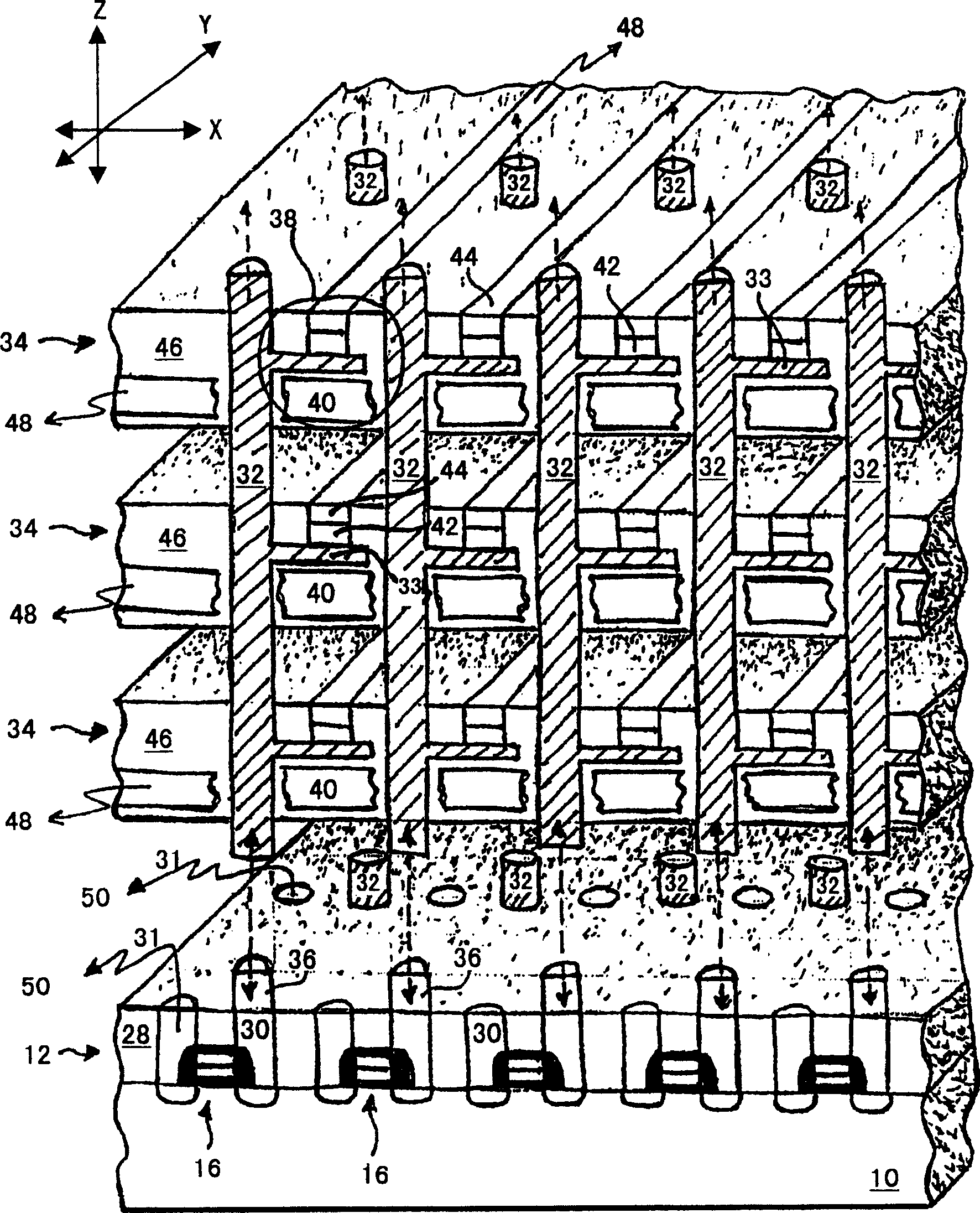
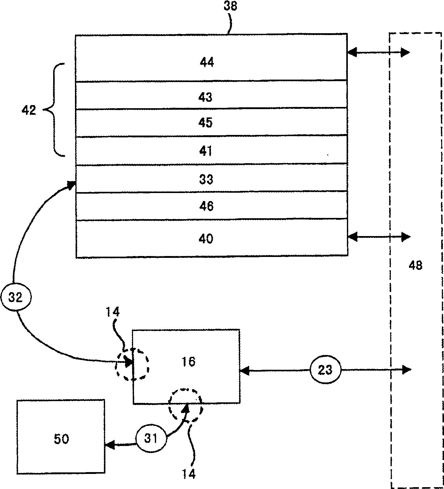
[0016] In the following detailed description, reference is made to various specific embodiments in which the invention may be practiced. These embodiments have been described in sufficient detail to enable those skilled in the art to practice the invention, and it is to be understood that other embodiments may be utilized and structural and electrical changes may be made without departing from the scope of the invention.
[0017] In the following description the terms "substrate" and "wafer" are used interchangeably and may include any semiconductor-based structure. It should be understood that structures include silicon, silicon-on-insulator (SOI), silicon-on-sapphire (SOS), doped and undoped semiconductors, epitaxial silicon layers supported by a base semiconductor substrate, and other semiconductors. structure. The semiconductor need not be silicon based. The semiconductor may be silicon-germanium, germanium or gallium arsenide. When referring to a substrate in the follo...
PUM
 Abstract
Description
Claims
Application Information
 - R&D Engineer
- R&D Manager
- IP Professional
- Industry Leading Data Capabilities
- Powerful AI technology
- Patent DNA Extraction
Browse by: Latest US Patents, China's latest patents, Technical Efficacy Thesaurus, Application Domain, Technology Topic.
© 2024 PatSnap. All rights reserved.Legal|Privacy policy|Modern Slavery Act Transparency Statement|Sitemap