Pixel circuit of display panel

A pixel circuit and display panel technology, applied in static indicators, nonlinear optics, instruments, etc., can solve the problems of display device damage and power consumption of display devices, and achieve the effect of reducing power consumption and switching frequency

Inactive Publication Date: 2009-04-01
SITRONIX TECH CORP
View PDF0 Cites 5 Cited by
  • Summary
  • Abstract
  • Description
  • Claims
  • Application Information

AI Technical Summary

Problems solved by technology

[0005] However, since the polarity of each adjacent pixel to which the data lines 20 ′ are coupled is different, when the scanning lines 10 ′ are turned on in sequence, the data lines 20 ′ need to reach the point The display effect of the conversion, and according to the output signals of the scanning lines 20' and the scanning lines 10', the positive and negative polarities are constantly switched, which consumes a lot of power of the display device (such as image 3 As shown), the power consumption of the point conversion system is mainly to overcome the load generated by the Indium Tin Oxide (ITP) layer, so the more frequent the polarity switching, the greater the power consumption
Furthermore, since these data lines 20' must constantly switch between positive and negative polarities, the display device is easily damaged.

Method used


Image

  • Pixel circuit of display panel
  • Pixel circuit of display panel
  • Pixel circuit of display panel

Examples


Embodiment Construction

[0034] In order to enable the examiner to have a further understanding and understanding of the structural features and achieved effects of the present invention, the preferred embodiments and accompanying drawings are used for detailed descriptions, as follows:

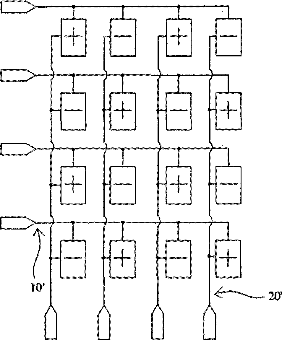
[0035] see Figure 4 , is a schematic structural diagram of a preferred embodiment of the present invention. As shown in the figure, the present invention is applied to a thin film transistor display (Thin Film Transistor Liquid Crystal Display, TFT-LCD), and the pixel circuit of the display panel of the present invention includes a plurality of pixels 10, a plurality of scanning lines 20 and a plurality of data lines 30, the These pixels 10 are arranged in rows and columns, and the polarity of each pixel in these pixels 10 is different from that of adjacent pixels 10, that is, the adjacent pixels of a positive polarity pixel 12 in these pixels 10 are all a negative polarity Sex Pixels14.

[0036] The scanning line...


PUM


Abstract

The invention relates to a pixel circuit of a display panel, which comprises plural pixels that are arranged in a line or row way, and the adjacent pixels have different polarities; plural scanning lines that are respectively coupled with the pixels on each row; and plural data lines that are coupled with the pixels according to the polarities of the pixels; therefore, by changing the layout structure of the pixels, the switching frequency of the polarity is reduced, thereby reducing the power consumption.

Description

technical field [0001] The present invention relates to a display panel, in particular to a pixel circuit of the display panel. Background technique [0002] The liquid crystal display of the prior art uses different voltage differences between the display electrode and the common electrode (common electrode) to control the rotation of the liquid crystal molecules to output different gray scales (gray scale), but the liquid crystal molecules cannot always be fixed in a certain state. , for example, the screen remains motionless, otherwise even if the driving voltage of the liquid crystal molecules is removed after a period of time, the liquid crystal molecules will no longer be able to rotate in response to changes in the electric field to form different gray scales due to changes in characteristics, so every once in a while It is necessary to restore the voltage to its original state to avoid changes in the characteristics of the liquid crystal molecules. [0003] Moreover...

Claims


Application Information

Patent Timeline
Patent Type & Authority Applications(China)
IPC IPC(8): G09G3/36G02F1/1362
Inventor 廖敏男
Owner SITRONIX TECH CORP
Why Eureka
Try Eureka