Hole inspection apparatus and hole inspection method using the same

一种检查装置、检查方法的技术,应用在孔检查装置和使用该孔检查装置的孔检查领域,能够解决花费时间等问题,达到减小试样损害的危险的效果

Inactive Publication Date: 2009-04-22
CEBT
View PDF1 Cites 7 Cited by
  • Summary
  • Abstract
  • Description
  • Claims
  • Application Information

AI Technical Summary

Problems solved by technology

[0005] However, the conventional hole inspection apparatus described above has a problem in that it takes a lot of time because of the use of the electron gun 2 that generates one electron beam.
That is, in the case where a large number of holes must be inspected, although the individual holes are accurately inspected, it takes a lot of time because the inspection has to be performed on the holes one by one

Method used


Image

  • Hole inspection apparatus and hole inspection method using the same
  • Hole inspection apparatus and hole inspection method using the same
  • Hole inspection apparatus and hole inspection method using the same

Examples


Embodiment Construction

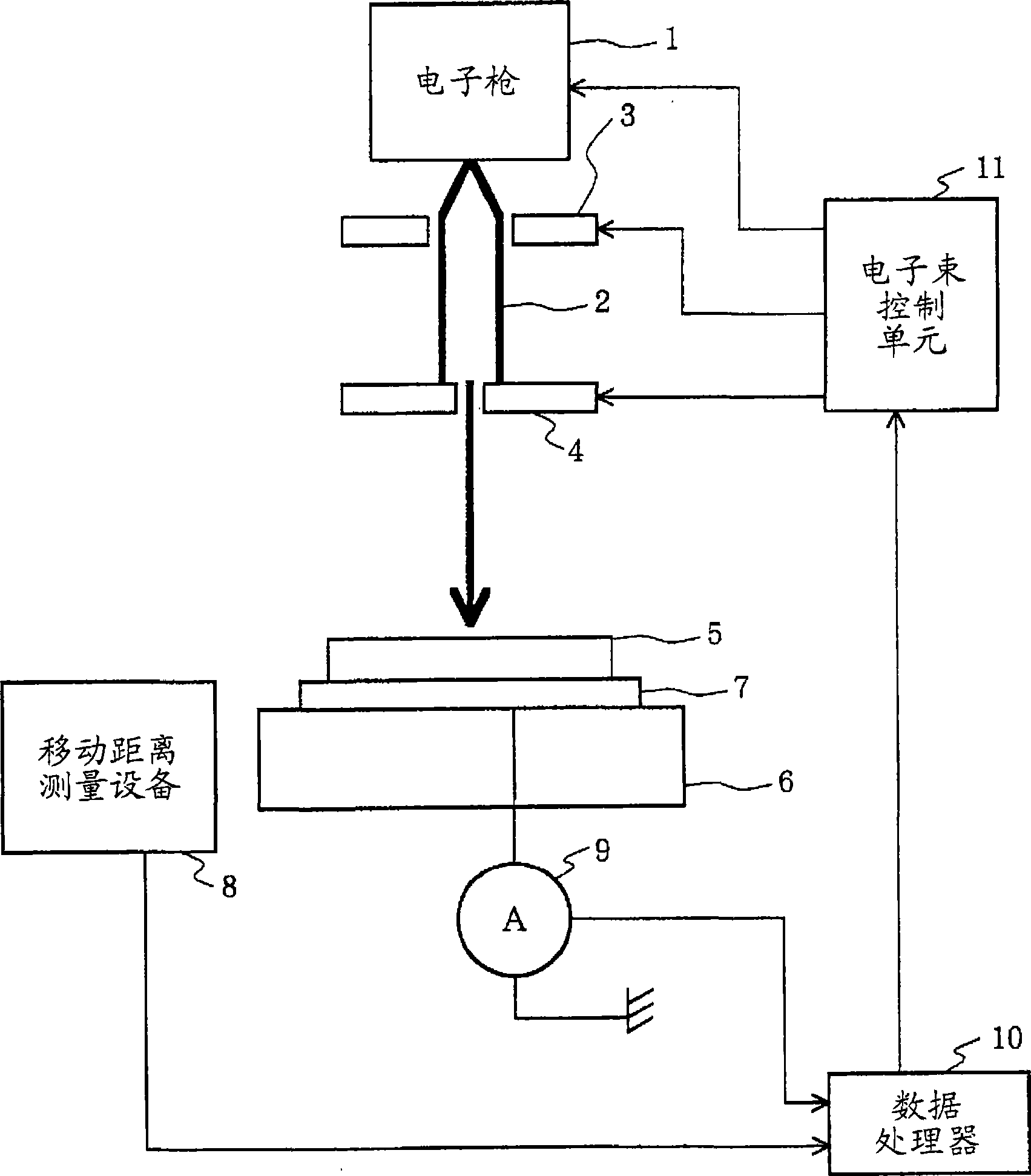
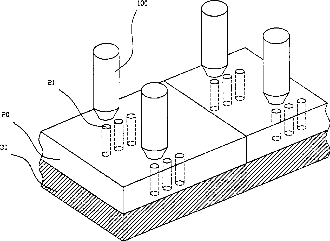
[0030] figure 2 A perspective view of the hole inspection device according to the present invention is schematically shown.

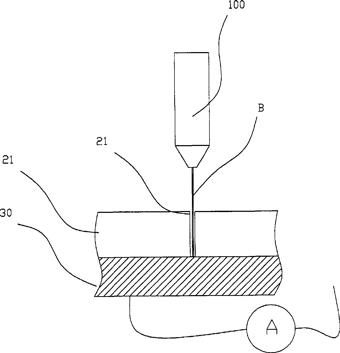
[0031] exist figure 2 In this example, four electron columns 100 were used as the electron beam irradiating means. For each description, each electron column 100 is described as radiating electron beams onto three holes 21 . The hole 21 is formed in the insulating layer 20 . The conductive layer 30 is located under the insulating layer 20 . In this case, three holes 21 to be inspected by the respective electron columns 100 are formed in the insulating layer 20 . Although the number of holes 21 and the size and shape of each hole have been set for the reason of describing the inspection device according to the present invention, the number of holes 21 and the size and shape of each hole may be determined differently.

[0032] Such as figure 2 As shown, the insulating layer 20 is divided into two regions, and the conductive layer 30 under the ins...


PUM


Abstract

Disclosed herein is an apparatus and a method for inspecting the via holes of a semiconductor device using electron beams. The apparatus includes electron beam irradiation means, a current measuring means, and a current measuring means and data processing means. The electron beam irradiation means radiate respective electron beams to inspect a plurality of inspection target holes. The current measuring means measures current, which is generated by irradiating the electron beams, radiated from the electron beam irradiation means, through a conductive layer located under the holes, or through the conductive layer and a separate detector. The data processing means processes data acquired through the measurement of the current measuring means.

Description

technical field [0001] The present invention relates generally to an apparatus and method for inspecting through-holes of semiconductor devices using electron beams, and more particularly to an apparatus and method for inspecting through-holes of semiconductor devices in a relatively short period of time, which enables multiple electron beam generating devices to The irradiated multiple electron beams pass through the semiconductor device, thereby measuring the current. Background technique [0002] Generally, a semiconductor device such as a memory has a contact hole or a via hole to electrically connect an active element formed at a lower portion of the contact hole or the via hole to a wiring layer formed at an upper portion of the contact hole or the via hole. Contact holes are formed by etching an insulating layer (eg, an oxide layer) from its surface to an underlying substrate using a reactive ion etching (RIE) process. In order to optimize the etching conditions, it ...

Claims


Application Information

Patent Timeline
Patent Type & Authority Applications(China)
IPC IPC(8): H01L21/66
CPCH01J2237/22H01J2237/281G01R31/307H01L22/12H01J2237/0635H01J2237/24564H01J37/28H01J2237/317H01J37/244H01J2237/24592H01J2237/244H01J2237/2817H01L22/14H01L22/00
Inventor 金浩燮
Owner CEBT
Why Eureka
Try Eureka