Direct image exposure device

An exposure device and image technology, which can be used in photolithography process exposure devices, microlithography exposure equipment, optics, etc., and can solve the problems of complex and expensive devices.

Inactive Publication Date: 2009-04-29
ADTEC ENG
View PDF3 Cites 9 Cited by
  • Summary
  • Abstract
  • Description
  • Claims
  • Application Information

AI Technical Summary

Problems solved by technology

[0011] Moreover, the devices used in the ab...

Method used


Image

  • Direct image exposure device
  • Direct image exposure device
  • Direct image exposure device

Examples


Embodiment Construction

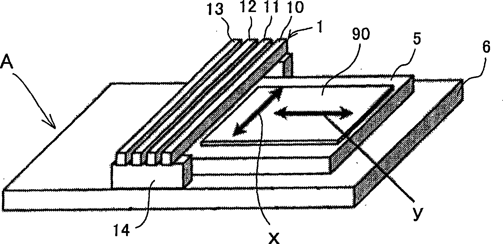
[0032] The present invention will now be described with reference to the accompanying drawings. figure 1 and 2 An embodiment of the direct image exposure of the present invention is shown.

[0033] The direct image exposure apparatus A has a base 6 on which the exposure head assembly 1 is disposed along the main scanning direction X, and a printed circuit board 90 on the exposure table 5 is disposed movable in the sub scanning direction Y.

[0034] The main scan of direct image exposure is performed by switching the illuminants such as LEDs of the exposure head assembly 1 , and the sub scan is performed by moving the exposure table 5 .

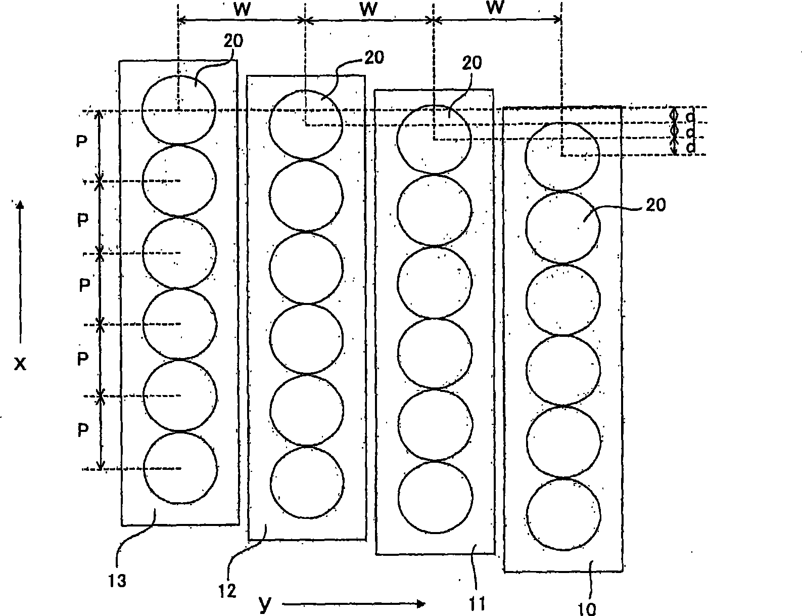
[0035] The exposure head assembly 1 has a plurality of exposure heads 10 , 11 , 12 , 13 . Although four exposure heads 10, 11, 12, 13 are provided in the present embodiment, the number can be changed as necessary.

[0036] The respective exposure heads 10 , 11 , 12 , 13 are arranged along the main scanning direction X, and the exposure head...


PUM


Abstract

The invention claims a direct image exposure device, characterized in that an exposure head assembly (1) has several exposure heads (10, 11, 12, 13) arranged parallel in a space W at a sub-scan direction Y; an exposure table (5) may move along the sub-scan direction Y under the exposure head assembly 1, may remove a printed circuit board (90) on the exposure table (5) under the exposure heads (10, 11, 12, 13), and may continuously expose the printed circuit board (90) by the exposure heads (10, 11, 12, 13); the exposure heads (10, 11, 12, 13) are provided with an array of LED (20) linearly arranged with the same space P; the LED (20) is arranged with space d at a main scan direction X among the exposure heads (10, 11, 12, 13), by which a same position of the sub-scan direction Y is repeatedly exposed, thereby implementing exposure of high position precision.

Description

technical field [0001] The present invention relates to a direct image exposure device for exposing an image directly onto a subject. Background technique [0002] The direct image exposure device utilizes an ultraviolet laser light source and a polygon mirror (references 1 and 2) or utilizes a combination of ultraviolet light emitted from a laser light source or a high-pressure mercury vapor tube and a digital micromirror device (DMD, digital micromirror device) (references 3 and 4) Exposure of an image onto an exposure object such as a printed circuit board. [0003] The former linearly scans laser light on an exposure object moving in a sub-scan direction through a polygon mirror that turns on / off a laser light source (main scan). The switching operation is performed by direct switching of a semiconductor laser device, or by analog switching of a solid-state laser through an acousto-optic modulator (AOM). [0004] The latter does not perform on-off control of the light ...

Claims


Application Information

Patent Timeline
IPC IPC(8): G03F7/20
CPCG03F7/70391G03F7/70383G03F7/70466
Inventor 中野幸夫
Owner ADTEC ENG
Why Eureka
Try Eureka