Methods to obtain low k dielectric barrier with superior etch resistivity
一种电介质阻挡、电介质层的技术,应用在涂层、电路、电气元件等方向,能够解决蚀刻选择性和阻挡性能损失等问题
- Summary
- Abstract
- Description
- Claims
- Application Information
AI Technical Summary
Problems solved by technology
Method used
Image

Examples
example 1
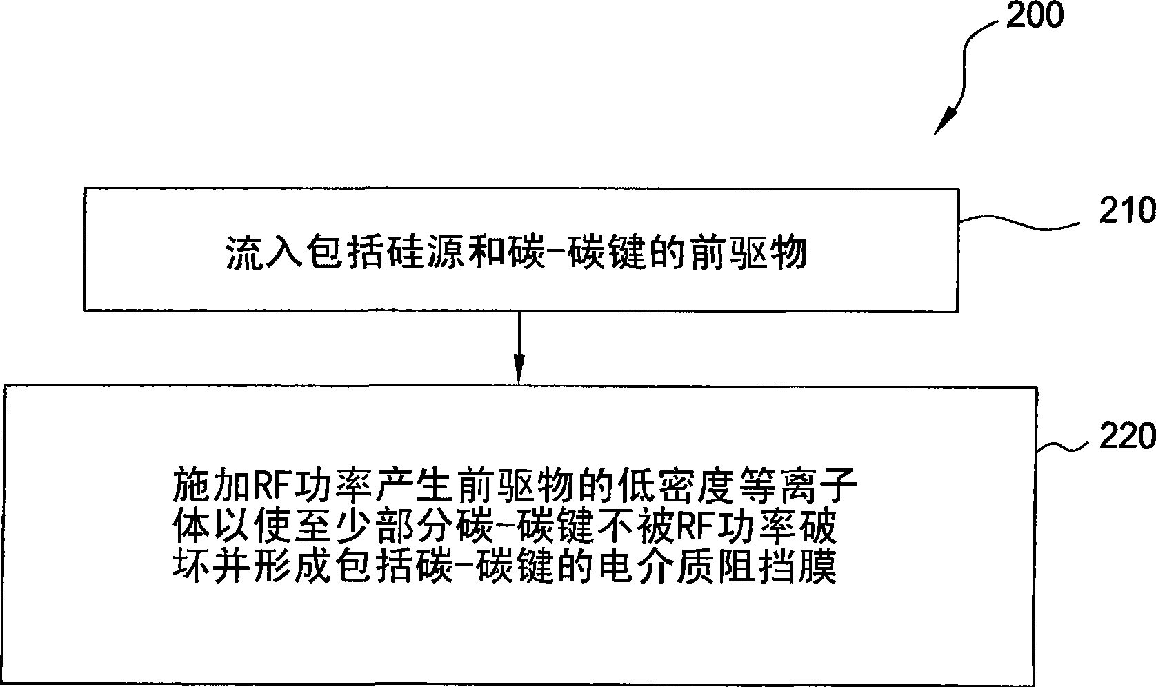
[0083] The PECVD deposition process used to deposit porous dielectric layers comprising silicon carbide uses compounds including trimethylsilane (TMS, (CH 3 ) 3 SiH) and ethylene (C 2 h 4 ) precursors of the composition. A carrier gas, such as helium, argon, nitrogen, or combinations thereof, is introduced into the processing chamber along with the precursors.
[0084] The ratio of TMS and ethylene is set such that the atomic ratio of carbon in the mixture is greater than 15%. In one embodiment, the ratio of ethylene to TMS is between about 0.5:1 and about 8:1. In another embodiment, the ratio of ethylene to TMS is between about 1:1 and about 4:1. The processing parameters are as follows:
[0085] Flow rate (including precursor and carrier gas): between about 5 seem and about 10,000 seem, wherein the flow rate of carrier gas can be between about 5 seem and about 10,000 seem.
[0086] Pitch: from about 200 mils to about 2000 mils;
[0087] Temperature: between about 100...
example 2
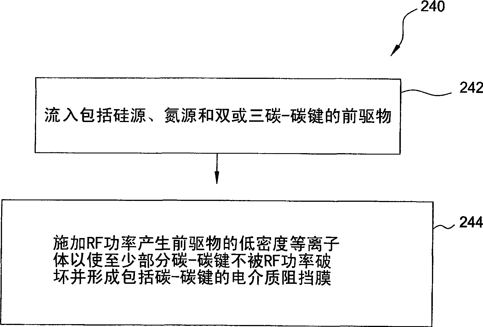
[0091] The PECVD deposition process used to deposit porous dielectric layers comprising silicon carbide uses compounds including trimethylsilane (TMS, (CH 3 ) 3 SiH), ethylene (C 2 h 4 ) and ammonia (NH 3 ) precursors of the composition. In one embodiment, the ratio of ethylene to TMS is between about 3:1 and about 5:1. The ratio of ammonia to TMS can be between about 1:10 to about 10:1. In another embodiment, the ratio of ammonia to TMS may be between about 1:4 and about 3:1. The processing parameters are as follows:
[0092] Flow rate (including precursor and carrier gas): between about 5 sccm and about 10,000 sccm, wherein the flow rate of the carrier gas can be between about 5 sccm and about 10,000 sccm.
[0093] Spacing: from about 200mm to about 2000mm;
[0094] Temperature: between about 100°C and about 550°C, or between about 200°C and about 350°C;
[0095] Chamber pressure: between about 10mTorr and one atmosphere;
[0096] RF Power: From about 15W to about ...
example 3
[0098] The PECVD deposition process used to deposit porous dielectric layers comprising silicon carbide uses compounds including trimethylsilane (TMS, (CH 3 ) 3 SiH) and ethylene (C 2 h 4 ) precursors of the composition. The processing conditions, including the ratio of TMS and ethylene, are set such that the atomic ratio of carbon is greater than 15%. In one embodiment, the ratio of ethylene to TMS is from about 1:1 to about 8:1, the flow rate of TMS / Northern precursor and carrier gas is from about 5 sccm to about 10,000 sccm, and the temperature is about 350°C. For these conditions, the chamber pressure is between about 10 mTorr and one atmosphere, the radio frequency (RF) power used to generate the plasma is between about 15 W and about 3,000 W, and the substrate set for supplying the precursors to the substrate being processed is The spacing between the base and the spray tip is from about 200 mils to about 2000 mils.
[0099] Advantages of barrier layers
[0100] Th...
PUM
 Abstract
Description
Claims
Application Information
 - R&D Engineer
- R&D Manager
- IP Professional
- Industry Leading Data Capabilities
- Powerful AI technology
- Patent DNA Extraction
Browse by: Latest US Patents, China's latest patents, Technical Efficacy Thesaurus, Application Domain, Technology Topic.
© 2024 PatSnap. All rights reserved.Legal|Privacy policy|Modern Slavery Act Transparency Statement|Sitemap