
Nonvolatile memory device and reading method thereof

A non-volatile storage and device technology, applied in the field of non-volatile storage devices and their reading, can solve problems such as influence

Inactive Publication Date: 2009-05-06
SK HYNIX INC
View PDF1 Cites 8 Cited by
  • Summary
  • Abstract
  • Description
  • Claims
  • Application Information

AI Technical Summary

Problems solved by technology

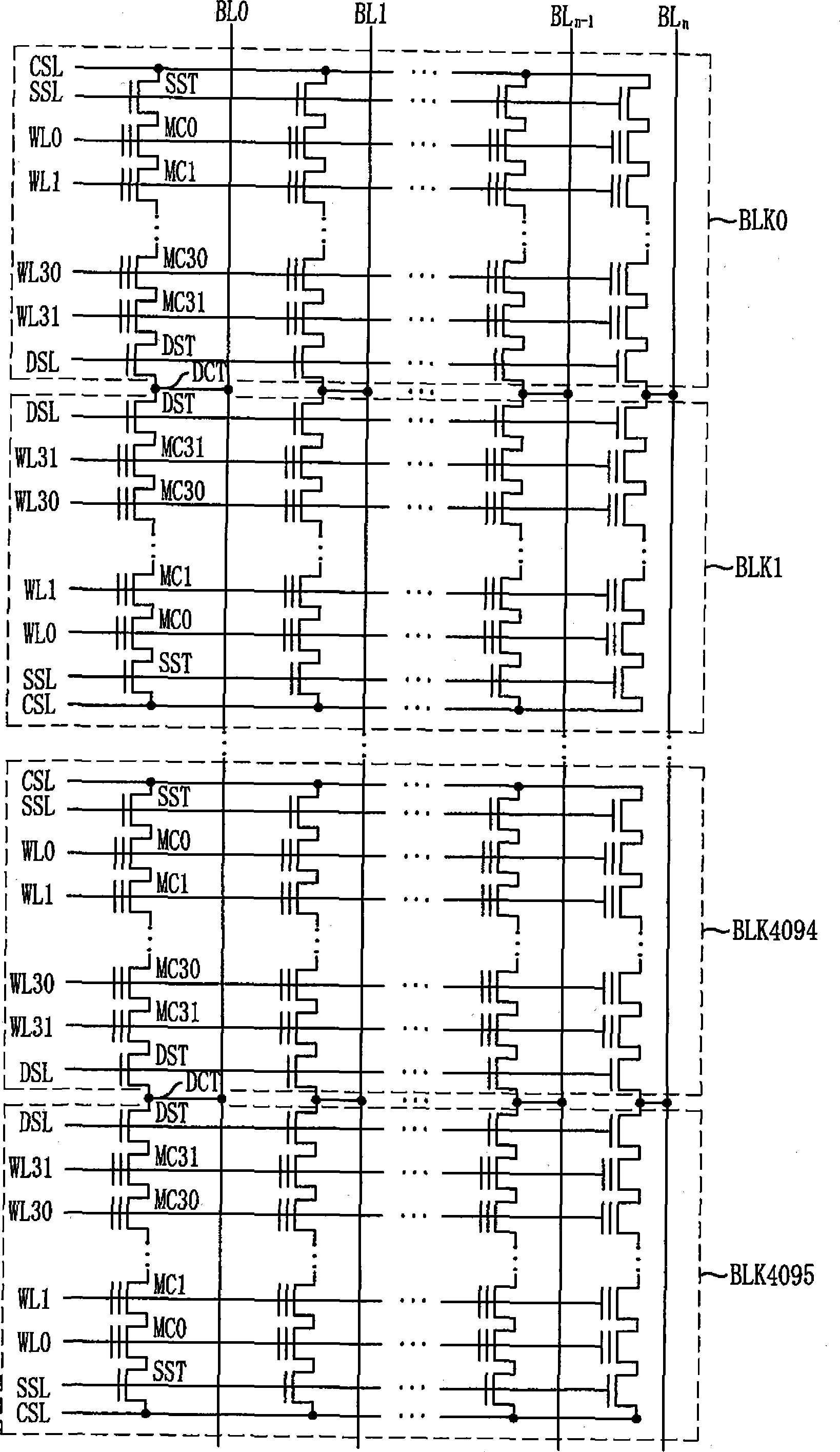
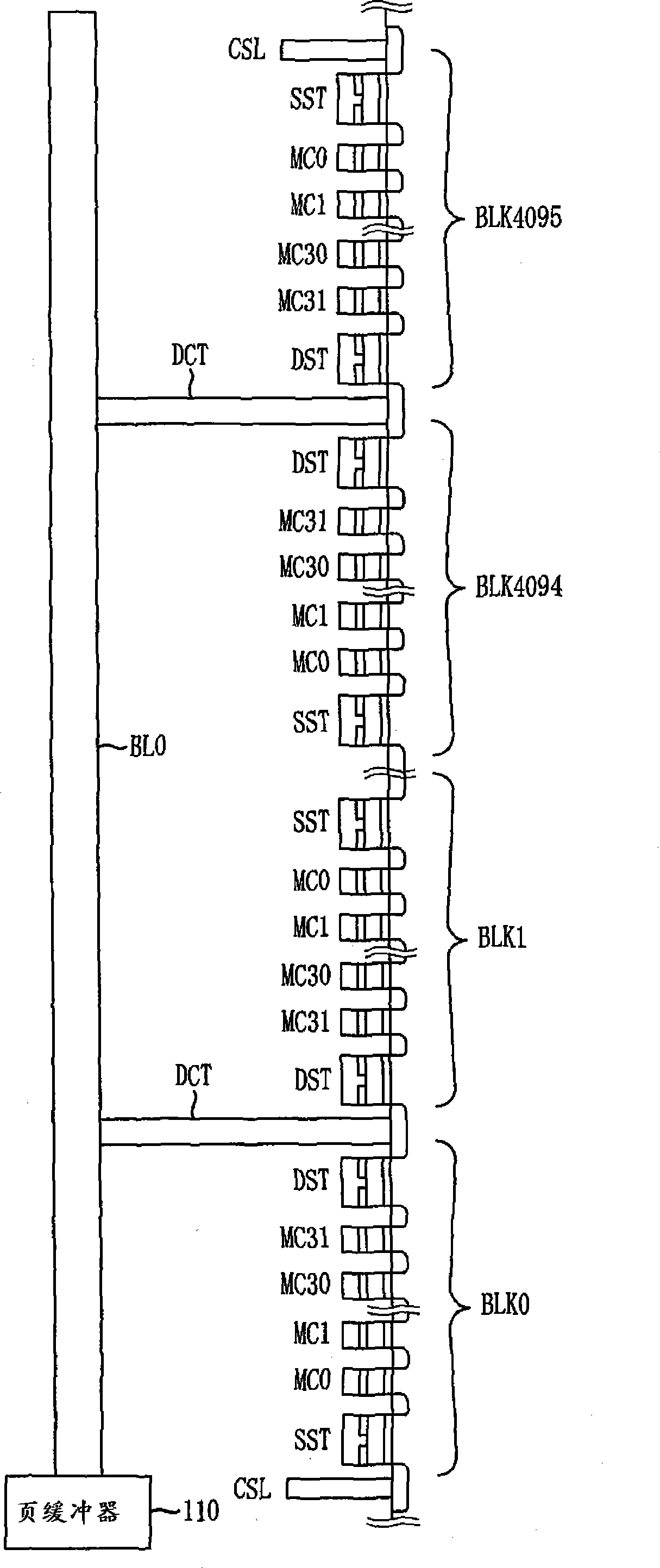
Therefore, in a page-by-page read operation, the leakage current due to the drain selection contact plug DCT of the unselected memory cell block may greatly affect the corresponding bit line

Method used


Image

  • Nonvolatile memory device and reading method thereof
  • Nonvolatile memory device and reading method thereof
  • Nonvolatile memory device and reading method thereof

Examples


Embodiment Construction

[0020] Hereinafter, a nonvolatile memory device and a reading method of the nonvolatile memory device according to the present invention will be described in detail with reference to the accompanying drawings. Like reference numerals in the drawings indicate like elements.

[0021] Figure 4 is a block diagram of a NAND-type flash memory device according to an embodiment of the present invention. Figure 5A with 5B yes Figure 4 The schematic circuit diagram of the blocks BLK0 ~ BLK4095 shown. Image 6 yes Figure 5A with 5B A cross-sectional view of blocks BLK0-BLK4095 connected to bit line BL0 is shown.

[0022] refer to Figure 4~6 , the memory cell array 200 of the NAND flash memory device is divided into 64 groups based on the cell blocks BLK0˜BLK4095. Accordingly, the memory cell array 200 is divided into 64 groups G0˜G63. The division into 64 groups is merely exemplary, and the number of divisions is not limited to this example. The number of divisions is deter...


PUM


Abstract

A nonvolatile memory device can improve its operation characteristic by reducing leakage current of a bit line in a read operation. The nonvolatile memory device includes a plurality of word lines, a plurality of main bit lines intersecting with the plurality of word lines, a plurality of cell blocks each including a plurality of cell strings, each of the cell strings including first and second select transistors and a plurality of memory cells, a plurality of sub bit lines commonly connected to the respective cell strings in same group, the cell blocks being grouped into a plurality of groups whose number is identical to or smaller than the number of the cell blocks, a plurality of group selectors configured to selectively connect the main bit lines to the sub bit lines of a selected group, and a plurality of page buffers configured to sense data of the memory cells through the main bit lines.

Description

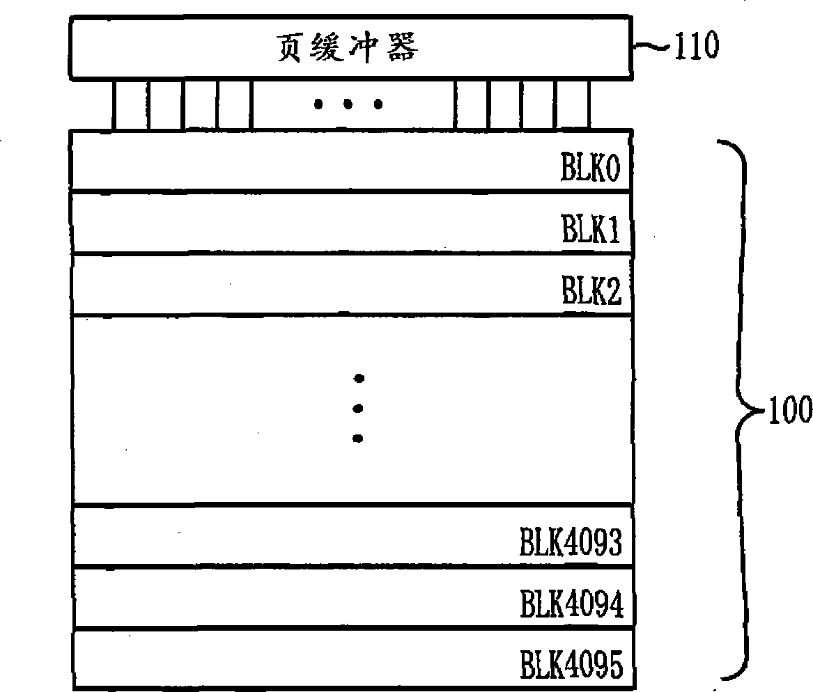
[0001] Cross References to Related Applications [0002] This application claims priority from Korean Patent Application No. 10-2007-0111199 filed on Nov. 1, 2007, the entire contents of which are hereby incorporated by reference. technical field [0003] The invention relates to semiconductor design technology, in particular to a non-volatile storage device and a reading method thereof. Background technique [0004] A NAND-type flash memory device is one of non-volatile memory devices. A NAND type flash memory device includes a plurality of cell strings each having a plurality of cells connected in series in a highly integrated manner. NAND flash memory is used in various fields, such as memory sticks, universal serial bus (USB, universal serial bus) drives, and hard disks. [0005] figure 1 is a block diagram of a conventional NAND-type flash memory device. figure 2 yes figure 1 The schematic circuit diagram of the blocks BLK0 ~ BLK4095 shown. image 3 yes figure ...

Claims


Application Information

Patent Timeline
IPC IPC(8): G11C16/08
CPCG11C16/0483G11C16/24G11C7/18G11C5/063G11C16/26
Inventor 尹太彦
Owner SK HYNIX INC
Learn More