Non-volatile memory device
一种非易失性存储、存储器件的技术,应用在非易失性存储应用的器件领域,能够解决非易失性存储器件亚阈值特性变差等问题
- Summary
- Abstract
- Description
- Claims
- Application Information
AI Technical Summary
Problems solved by technology
Method used
Image

Examples
Embodiment Construction
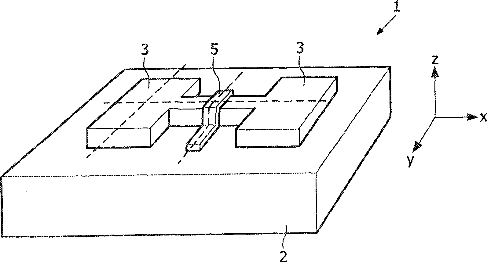
[0043] figure 1 A perspective layout of an embodiment of a finFET-based non-volatile memory device is shown.
[0044]The finFET structure F is located in a monocrystalline silicon layer 1 on an insulating layer 2, for example a silicon dioxide layer or a BOX (Buried Oxide) layer of an SOI (SOI: Silicon on Insulator) wafer.
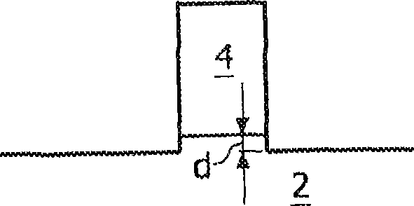
[0045] The finFET structure F comprises source and drain regions 3, S, D and (relatively narrow) lines or fins 4 which lie between and connect the source and drain regions . The source, drain and fin regions 3, S, D, 4 are made of silicon semiconductor material. The fin region 4 has a substantially rectangular cross-section comprising side wall portions and a top portion.
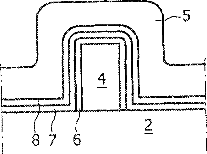
[0046] The gate 5 is located on the insulating layer 2 between the source and drain regions 3 and extends over the fins 4 in a Y direction which is substantially perpendicular to the length direction X of the fins 4 . The gate 5 is separated from the fin 4 by a charge trapping stack...
PUM
 Abstract
Description
Claims
Application Information
 - R&D
- Intellectual Property
- Life Sciences
- Materials
- Tech Scout
- Unparalleled Data Quality
- Higher Quality Content
- 60% Fewer Hallucinations
Browse by: Latest US Patents, China's latest patents, Technical Efficacy Thesaurus, Application Domain, Technology Topic, Popular Technical Reports.
© 2025 PatSnap. All rights reserved.Legal|Privacy policy|Modern Slavery Act Transparency Statement|Sitemap|About US| Contact US: help@patsnap.com