Method for producing a semiconductor component

A semiconductor and component technology, which is applied in the fields of semiconductor/solid-state device manufacturing, semiconductor devices, and semiconductor/solid-state device components, etc., can solve problems such as component damage, and achieve the effect of reducing danger and avoiding the risk of damage.

Inactive Publication Date: 2009-05-20
SEMIKRON ELECTRONICS GMBH & CO KG
View PDF3 Cites 10 Cited by
  • Summary
  • Abstract
  • Description
  • Claims
  • Application Information

AI Technical Summary

Problems solved by technology

[0005] The disadvantage of such known sintering methods by means of mechanical pressure is that they can generally only form one sintered connection at a time and / or there is a risk of component damage, especially during the joining of semiconductor components.

Method used


Image

  • Method for producing a semiconductor component
  • Method for producing a semiconductor component
  • Method for producing a semiconductor component

Examples


Embodiment Construction

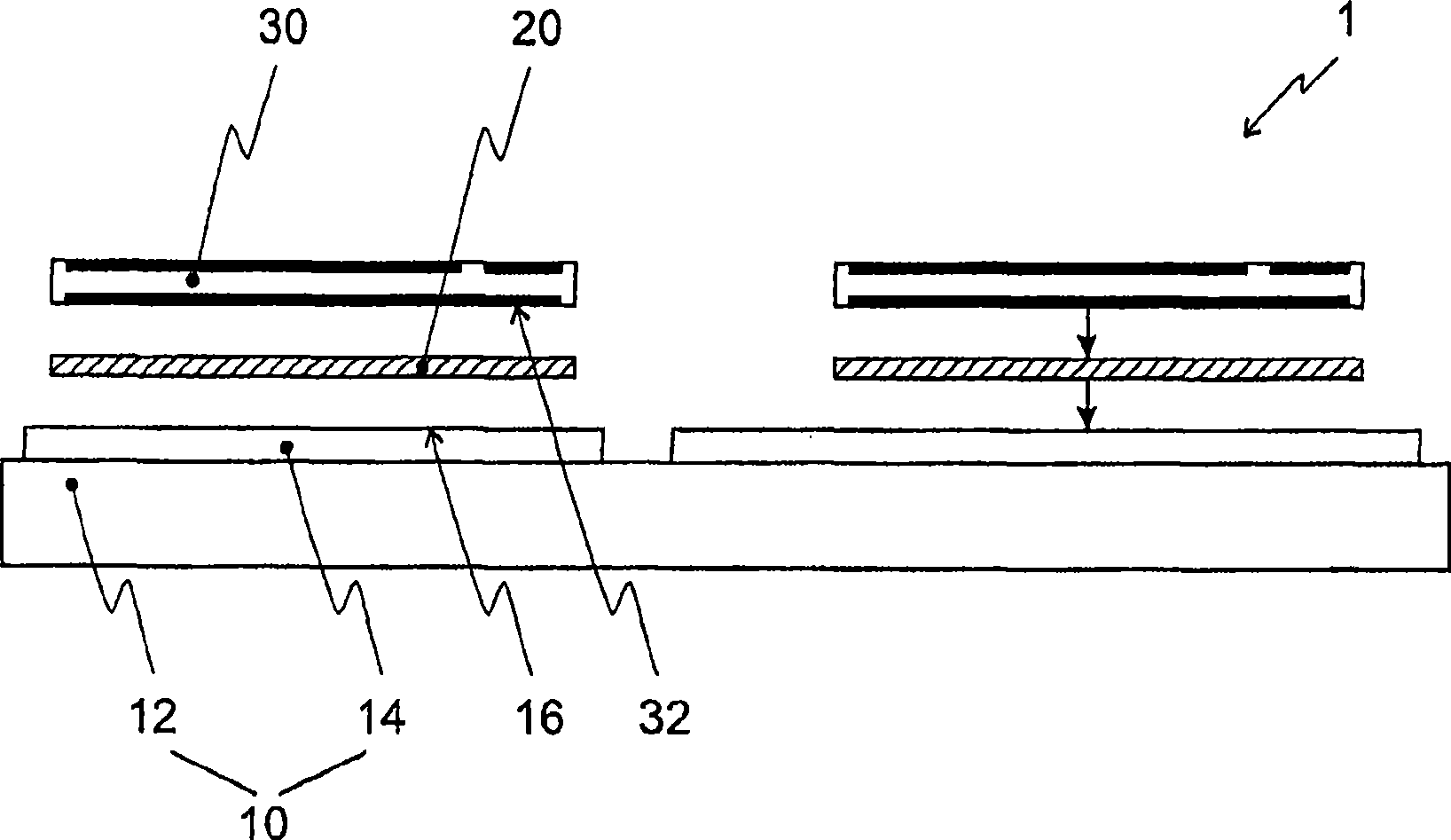
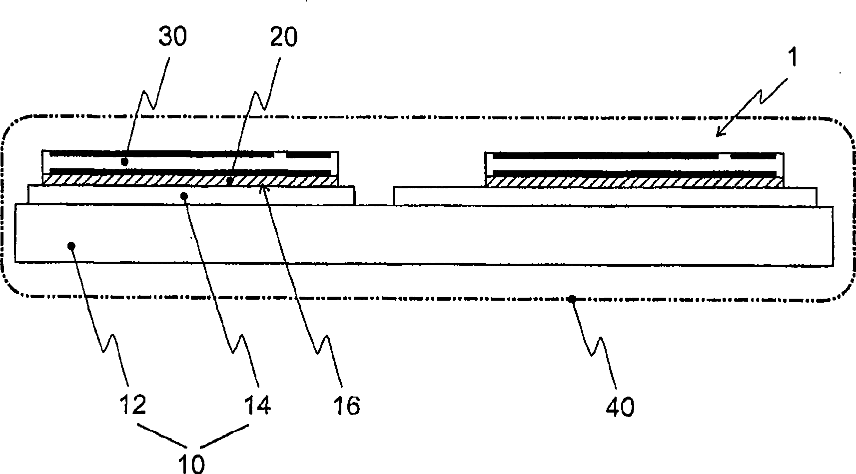
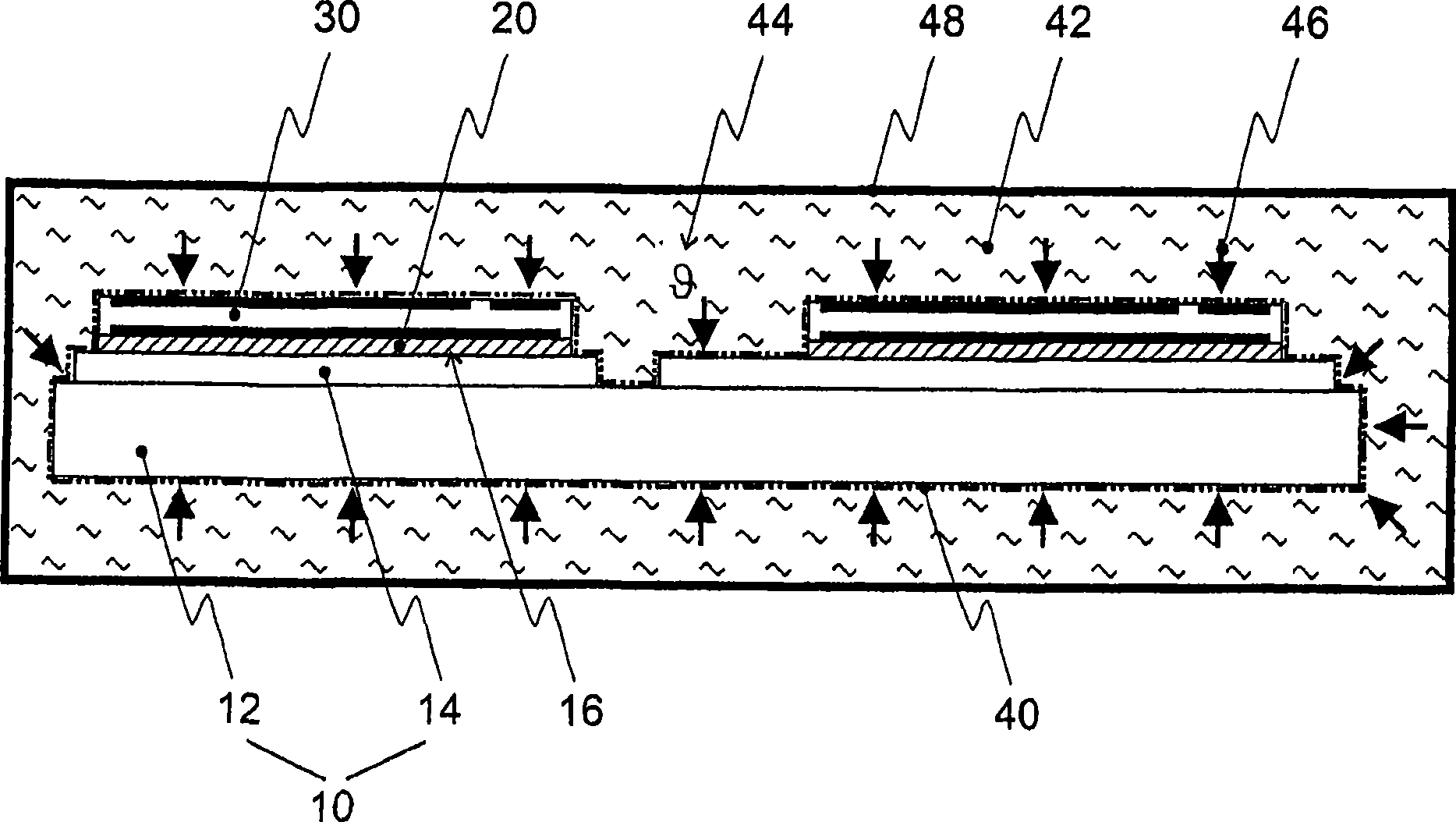
[0021] figure 1 The first step of the semiconductor component manufacturing method according to the present invention is shown. The connecting device is designed here as an electrically insulating substrate 10 which, according to the prior art, has an insulating base body 12 and a plurality of conductor tracks 14 arranged on at least one main surface and contact areas 16 formed thereon. In the case of sinter bonding, according to the prior art, it is advantageous for the contact surface 16 to have a noble metal surface. The substrate 10 is preferably designed as a conventional printed circuit board, IMS (isolated metal substrate) or DBC (direct copper connection) substrate. The exemplary embodiment of the connection means as substrate 10 does not limit the generality of the above description. It is likewise conceivable for the connection unit (see FIGS. 4 to 6 ) to be used to bond a substrate or one or more semiconductor components for internal and / or external contacting.

...


PUM


Abstract

The invention relates to a method for manufacturing semiconductor subassemblies and comprises the flowing main procedures: forming a structure which is provided with at least one semiconductor member, at least one connecting device, and at least one variety of conjugation agent arranged between the semiconductor member and the connecting device. The structure is partially or wholly packed, and the at least one semiconductor member and the at least one connecting device are unified into an entity.

Description

technical field [0001] The invention relates to a method for the production of semiconductor components, for example components of power semiconductor modules. According to the prior art, such a power semiconductor module has a housing, a substrate with power semiconductor components, and load and auxiliary connection units. The semiconductor component referred to below refers, for example, to an assembly as a component part of a power semiconductor module, the module comprising a substrate and a semiconductor component integrally connected with the substrate material, or a connecting unit in which the semiconductor component and the material are integrally connected, or comprising their combination. This includes not only substrates, but also connection units in the sense of connection means. Background technique [0002] In order to manufacture such semiconductor components, soldering and sintering methods are known in the prior art. DE19911887C1 discloses a reflow weld...

Claims


Application Information

Patent Timeline
Patent Type & Authority Applications(China)
IPC IPC(8): H01L21/50H01L21/60H01L21/603H01L21/56H01L25/00H01L23/488H01L23/31
CPCH01L2224/83136H01L24/83H01L23/3121H01L24/40H01L2924/12044H01L2224/83101H01L21/56H01L2224/293H01L2924/01015H01L24/92H01L23/4985H01L2924/01047H01L23/49833H01L2924/01006H01L2224/8384H01L25/072H01L2224/83801H01L2224/29339H01L2224/2732H01L2224/83192H01L2224/9221H01L2224/751H01L2924/01005H01L2924/01013H01L2224/29294H01L2924/014H01L2924/01029H01L23/3735H01L25/50H01L2224/24226H01L24/27H01L24/32H01L2224/2402H01L2924/01068H01L2224/75315H01L24/75H01L2224/40225H01L2224/371H01L24/37H01L2224/84801H01L24/50H01L24/84H01L2224/06181H01L2224/0603H01L2924/00H01L2924/00014
Inventor T·斯托克梅尔H·海尔布伦尔C·戈布尔
Owner SEMIKRON ELECTRONICS GMBH & CO KG
Why Eureka
Try Eureka