Pixel structure and preparation method thereof, array substrate and display device

A pixel structure and insulating layer technology, which is applied in semiconductor/solid-state device manufacturing, optics, instruments, etc., can solve problems such as process time increase, follow-up process problems, gate insulating layer 2 breakage, etc., to reduce process steps and improve production Efficiency, cost-saving effect

Active Publication Date: 2016-03-23
BOE TECH GRP CO LTD +1
View PDF4 Cites 5 Cited by
  • Summary
  • Abstract
  • Description
  • Claims
  • Application Information

AI Technical Summary

Problems solved by technology

During the fabrication of thin film transistors, due to the thickness of the gate 4 (usually left and right), when the gate insulating layer 2 is deposited on the gate 4, a relative level difference is formed at the overlap between the gate 4 and the gate insulating layer 2, which makes the gate insulating layer 2 prone to breakage, resulting i

Method used


Image

  • Pixel structure and preparation method thereof, array substrate and display device
  • Pixel structure and preparation method thereof, array substrate and display device
  • Pixel structure and preparation method thereof, array substrate and display device

Examples


Embodiment 1

[0054] This embodiment provides a pixel structure and its corresponding preparation method. The preparation method is simple, and the prepared pixel structure has high yield and good performance.

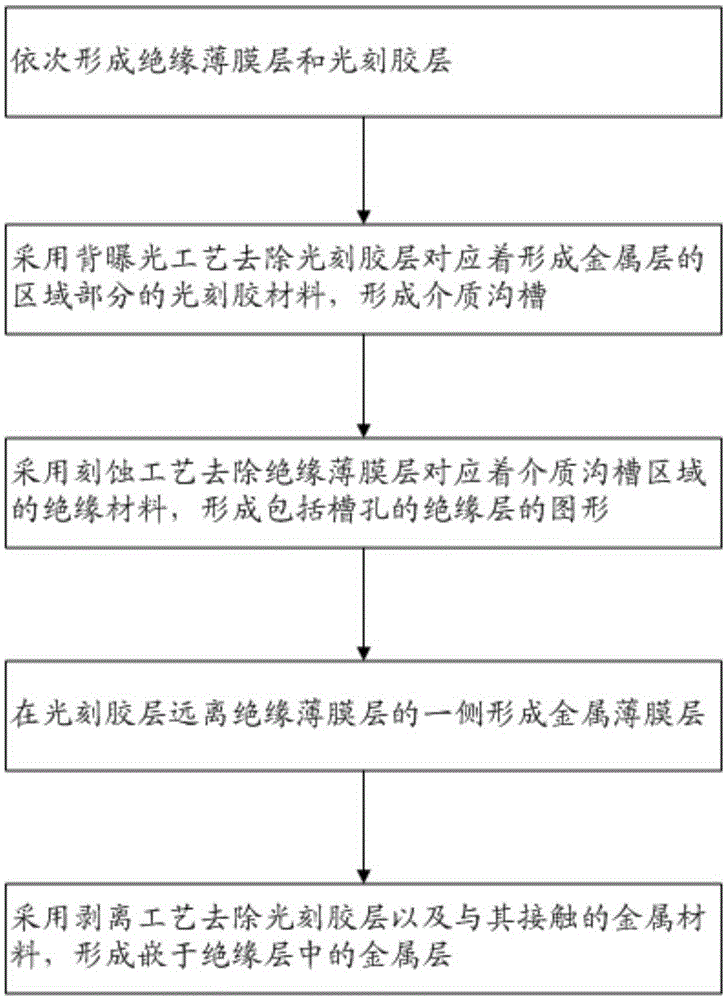
[0055] A method for preparing a pixel structure, comprising the steps of forming an insulating layer and forming a metal layer embedded in the insulating layer, including: forming a transparent medium layer, and using a back exposure process and a lift-off process to process the transparent medium layer, forming a The pattern of the insulating layer and the pattern of the metal layer embedded in the insulating layer; wherein, the insulating layer is provided with a slot for embedding the metal layer, the shape of the slot is suitable for the shape of the metal layer, and the area of ​​the slot is equal to The area of ​​the metal layer and the depth of the slot hole are equal to the thickness of the metal layer.

[0056] A pixel structure corresponding to the above preparation method...

Embodiment 2

[0084] This embodiment provides a pixel structure and its corresponding preparation method. The preparation method is simple, and the prepared pixel structure has high yield and good performance.

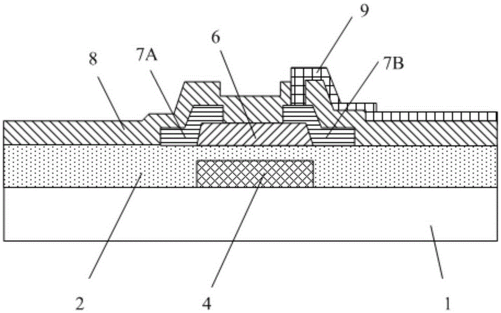
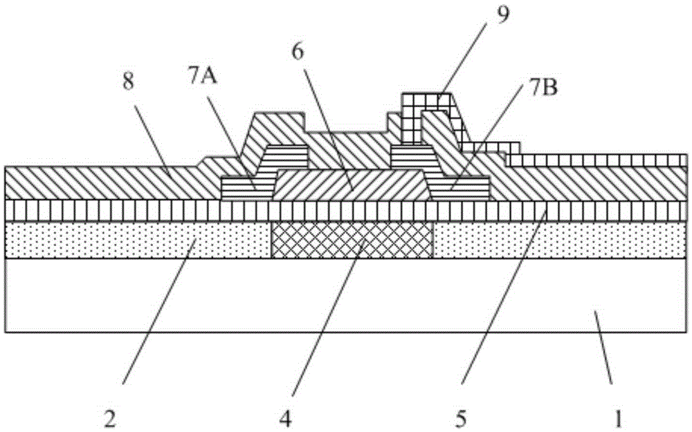
[0085] This embodiment also takes the formation of the gate insulating layer 2 and the gate 4 embedded in the gate insulating layer 2 in the top-gate thin film transistor as an example to describe the preparation process in detail. Compared with Example 1, the difference in the preparation method of this pixel structure is that when forming the dielectric trench 31 of the photoresist layer 3, in the back exposure process, a semi-permeable film mask is used to form two waists as the outer Convex curved trapezoidal shape.

[0086] Further preferably, the center of the exposure light source corresponds to the center of the dielectric trench 31 to be formed, and the cross-sectional shape of the dielectric trench 31 is an isosceles trapezoid whose two waists are convex arcs.

[0087] In...

Embodiment 3

[0090] This embodiment provides a pixel structure and its corresponding preparation method. The preparation method is simple, and the prepared pixel structure has high yield and good performance.

[0091] Compared with Embodiments 1 and 2, the difference in the preparation method of the pixel structure is that this embodiment takes the formation of the passivation layer 8 under the top-gate thin film transistor and the pixel electrode 9 embedded in the passivation layer 8 as an example. Describe the preparation process.

[0092] In the pixel structure of this embodiment, the pixel structure includes a thin film transistor, and a pixel electrode 9 and a passivation layer 8 located below the thin film transistor. Here, the insulating layer is the passivation layer 8 , and the metal layer is the pixel electrode 9 layer. According to the principle of straight-line propagation of light, in order to ensure the effectiveness of the back exposure process, the passivation layer 8 and ...


PUM


Abstract

The invention belongs to the technical field of display, and relates to a pixel structure and a preparation method thereof, an array substrate and a display device. The preparation method of the pixel structure comprises the steps of forming an insulation layer and forming a metal layer embedded into the insulation layer and specifically comprises the steps of forming a transparent medium layer, adopting a back exposure process and a stripping process to treat the transparent medium layer, and forming a graph comprising the insulation layer and a graph of the metal layer embedded into the insulation layer; the insulation layer is internally provided with a slotted hole in which the metal layer is embedded, the shape of the slotted hole is adaptive to that of the metal layer, the area of the slotted hole is equal to that of the metal layer, and the depth of the slotted hole is equal to the thickness of the metal layer. According to the preparation method of the pixel structure, the back exposure process and the stripping process are combined, so that the time lag between the two periods of time of forming the insulation layer and forming the metal layer embedded into the insulation layer is effectively avoided, the process is simple and the production efficiency is effectively improved.

Description

technical field [0001] The invention belongs to the field of display technology, and in particular relates to a pixel structure and a preparation method thereof, an array substrate and a display device. Background technique [0002] With the development of display technologies, liquid crystal display devices (Liquid Crystal Display, LCD for short) and OLED display devices (Organic Light Emission Display, organic electroluminescence) have become mainstream display devices at present. The liquid crystal display device is currently the most widely used type of flat panel display device, and its main component is a liquid crystal panel. The liquid crystal panel mainly includes a color filter substrate, an array substrate, and a liquid crystal disposed between them. [0003] The array substrate is an important part of the LCD display device, which includes a thin film transistor (ThinFilmTransistor, referred to as TFT) and a pixel electrode connected to the thin film transistor. ...

Claims


Application Information

Patent Timeline
IPC IPC(8): H01L21/336H01L29/786H01L29/423H01L27/12H01L27/32G02F1/1362
CPCG02F1/1362H01L27/12H01L29/42364H01L29/42384H01L29/66742H01L29/786H10K59/00H01L21/0274H01L21/31144H01L29/78636H01L27/124H01L27/1288G02F1/1368H01L21/28H01L21/768H01L21/84H01L27/1214H01L29/49
Inventor 万云海杨成绍韩领宋博韬
Owner BOE TECH GRP CO LTD
Why Eureka
Try Eureka