Wafer jig having identification mark

A technology for identifying marks and chips, which is applied in the manufacture of electrical components, electrical solid devices, semiconductor/solid devices, etc., and can solve problems such as not easy to obtain, difficult to always hold, chip damage, etc.

Active Publication Date: 2019-01-01
DISCO CORP
View PDF3 Cites 6 Cited by
  • Summary
  • Abstract
  • Description
  • Claims
  • Application Information

AI Technical Summary

Problems solved by technology

[0007] However, since the processing equipment manufacturer is not a wafer manufacturer, it is not easy to obtain various wafers, the wafer may be damaged when adjusting the identification mark reading mechanism, and it is difficult to always hold wafers with various identification marks.

Method used


Image

  • Wafer jig having identification mark
  • Wafer jig having identification mark
  • Wafer jig having identification mark

Examples


Embodiment Construction

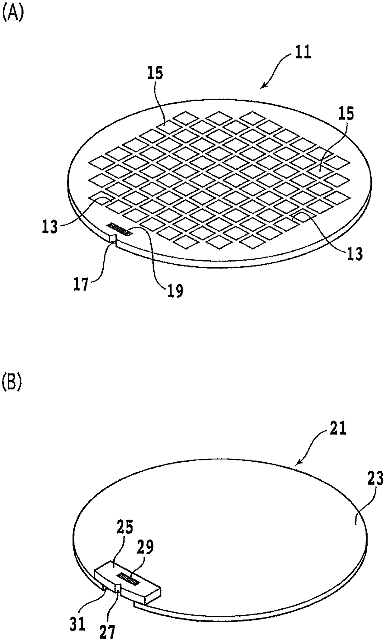
[0024] Hereinafter, embodiments of the present invention will be described in detail with reference to the drawings. when referring to figure 1 (A) shows a perspective view of a device wafer 11 with an identification mark. The device wafer 11 is typically a semiconductor wafer made of silicon, and devices 15 such as ICs and LSIs are formed in regions divided by a plurality of dividing lines (streets) 13 formed in a lattice.

[0025] A notch 17 indicating the crystal orientation of the device wafer 11 is formed on the outer periphery of the device wafer 11 . An identification mark (ID mark) 19 is formed adjacent to the notch 17 . The identification mark 19 is formed of numbers, characters, barcodes or combinations thereof. The identification mark 19 is a mark for identifying the type of the device 15 and information for each wafer, and the same identification mark 19 is given to all the device wafers 11 of the same batch.

[0026] when referring to figure 1 (B) is a perspe...


PUM


Abstract

The invention provides a wafer jig having an identification mark capable of being used for identifying adjustment of a reading mechanism. Disclosed herein is a wafer jig with an identification mark for use in inspecting the function of an identification mark reading mechanism for reading an identification mark on a device wafer. The wafer jig includes a wafer piece cut from a region of a device wafer where an identification mark is formed, and a circular plate having the same diameter as the device wafer. The wafer piece is fixed to the circular plate such that the identification mark on the wafer piece is positionally aligned with the identification mark on the device wafer.

Description

technical field [0001] The present invention relates to a wafer jig with an identification mark, which is used for function verification of an identification mark reading mechanism that reads an identification mark formed on a device wafer. Background technique [0002] For various wafers such as silicon, SiC, and sapphire on which various devices such as semiconductor devices and LEDs are formed, in order to identify the type of device of each wafer, dimensional information such as the thickness of the wafer, the interval between streets, and processing conditions, etc. Information, identification marks are formed by characters or barcodes near the periphery of the front or back of the wafer. [0003] Wafer identification marks are read by identification mark reading mechanisms provided in various processing devices, and are used to confirm which type of wafer is loaded into the processing device (for example, refer to Patent Document 1). [0004] Where the identification ...

Claims


Application Information

Patent Timeline
Patent Type & Authority Applications(China)
IPC IPC(8): H01L21/67H01L23/544
CPCH01L21/67294H01L23/544H01L21/67092H01L21/67253H01L21/67282H01L21/02021H01L2223/54493
Inventor 周忠
Owner DISCO CORP
Why Eureka
Try Eureka