High-efficiency heat-dissipating luminous high-power LED packaging structure

A LED packaging, high-power technology, applied in the direction of electrical components, circuits, semiconductor devices, etc., can solve the problems of reduced light output, increased chip temperature, and accelerated light attenuation of devices

Inactive Publication Date: 2009-05-20
王海军
View PDF2 Cites 20 Cited by
  • Summary
  • Abstract
  • Description
  • Claims
  • Application Information

AI Technical Summary

Problems solved by technology

Insufficient heat dissipation, resulting in an increase in the temperature of the LED chip, resulting in accelerated light attenuation of the device
Due to the aging of epoxy resin, yellowing will also reduce the light output

Method used


Image

  • High-efficiency heat-dissipating luminous high-power LED packaging structure
  • High-efficiency heat-dissipating luminous high-power LED packaging structure

Examples


Embodiment 1

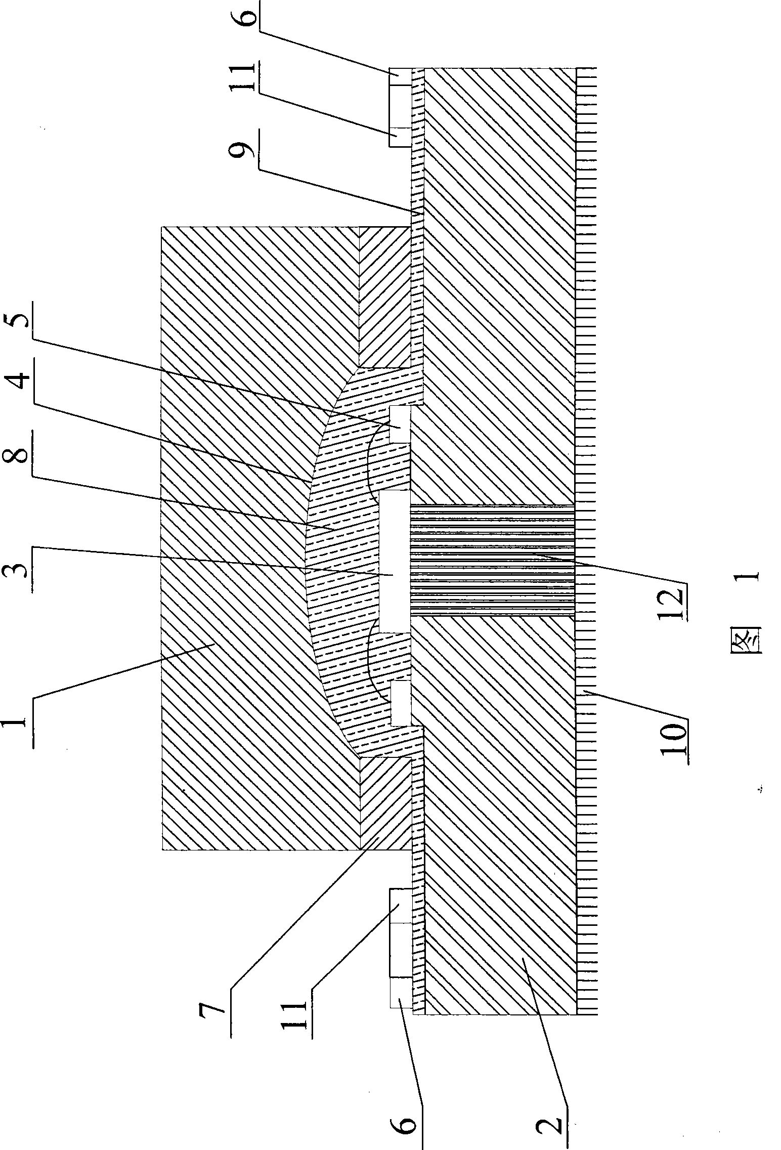
[0042] The lens 1 is a cuboid plate with a length of 3-10mm, a width of 2-9mm and a thickness of 1-5mm. In the crystal crystal lens 1, there is a mounting recess 4 in the center of the body of the lens 1, and the outer diameter of the mounting recess 4 is based on the standard not greater than the body of the lens 1. This mounting recess 4 is used to place the LED light-emitting chip 3, and During the encapsulation process, it is used to inject the cavity of silica gel 8.

[0043] The substrate 2 is a plate body of 3-14mm, 2-9mm wide, and 1-10mm thick. On the body of the crystal crystal substrate 2, there are different positive and negative light-emitting electrodes 5 formed on the substrate 2 according to different needs. The negative light-emitting electrode 5 is an electrode connected to the LED light-emitting chip 3. There are positive and negative connection electrodes 6 connected to the external power supply on the body of the crystal crystal substrate 1, and the electri...

Embodiment 2

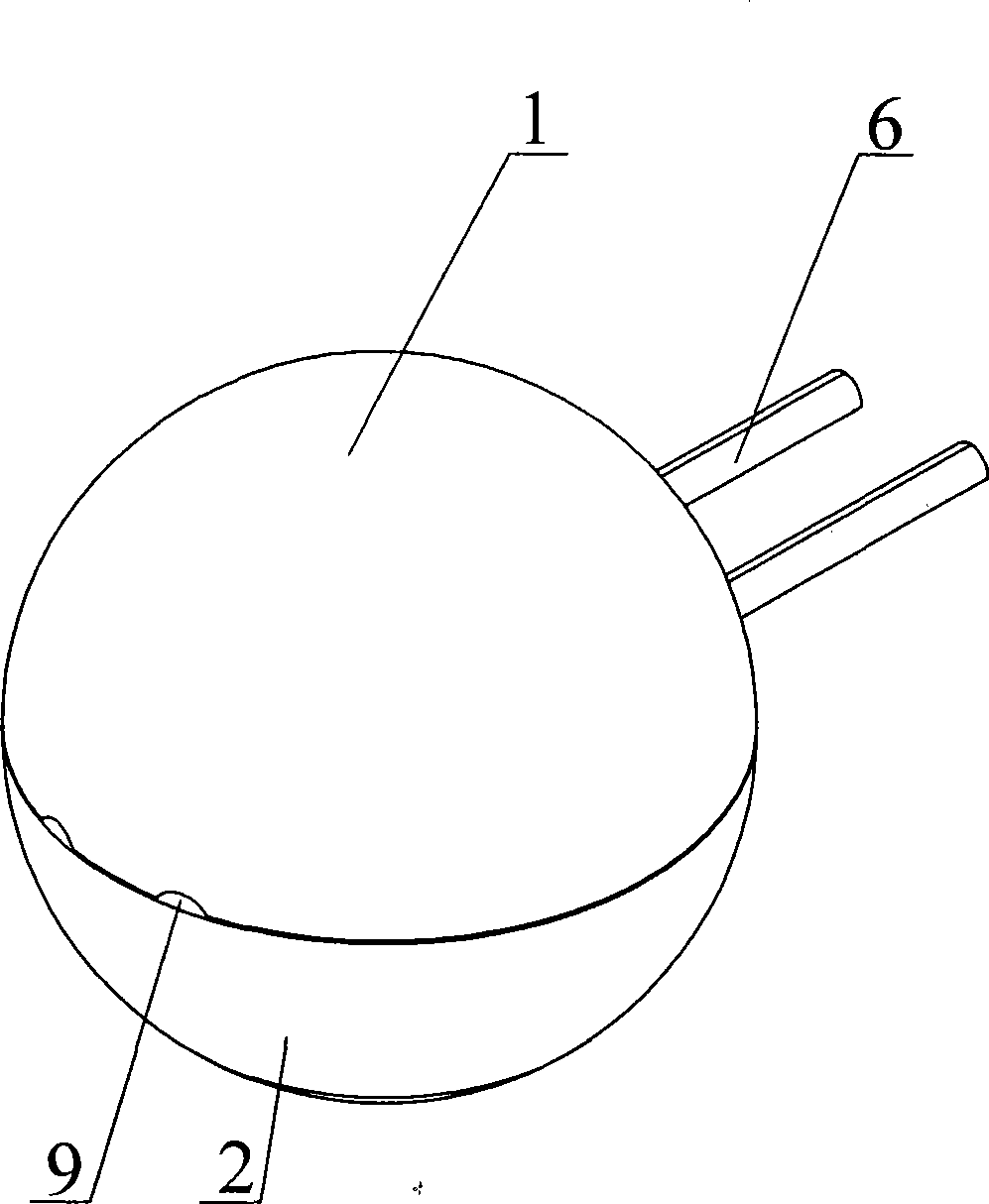
[0047] Both the lens 1 and the substrate 2 are hemispherical, and two ditches are opened on the upper surface of the substrate 2 through its body, and the ditch on one side of the LED light-emitting chip 3 forms a glue filling channel 9, and the ditch on the other side of the LED light-emitting chip 3 is formed to facilitate The foot-like connection is the channel into which the electrode 6 is inserted.

[0048] According to the above packaging scheme, the shape of the crystal substrate and the crystal lens 1 can be a hemisphere, and the plane of the hemisphere used as the substrate 2 has a light-emitting electrode 5 . Where the light-emitting electrode 5 is connected to the external power supply, there is a concave ditch according to the connection electrode 6, which is used as an insertion hole for connecting the legs with the external power supply, and this group of ditch is parallel to both sides of the LED light-emitting chip 3. The appearance of the crystal lens is a hem...


PUM


Abstract

The invention relates to a high-power LED packaging structure which radiates heat and illuminates efficiently and comprises a lens, a substrate and an LED luminous chip, wherein the lens is fixed on the upper surface of the substrate; the lower surface of the lens is provided with a raised mounting dent; the LED luminous chip is arranged on the upper surface of the substrate and is buckled and covered by the mounting dent; the upper surface of the substrate buckled and covered by the mounting dent is provided with a positive luminescence electrode and a negative luminescence electrode; the luminous electrodes are connected with the LED luminous chip through metal wires; the upper surface of the substrate is provided a positive connecting electrode and a negative connecting electrode which are connected with the luminous electrodes; the lower surface of the lens on the outer side of the mounting dent and the upper surface of the substrate are adhered through an annular adhesive layer; and a cavity formed by inner holes of the adhesive layer and the mounting dent is filled with silica gel; The substrate is provided with a gel-filling passage which is communicated with the cavity formed by inner holes of the adhesive layer and the mounting dent; and the lens and the substrate are made from quartz crystal. The high-power LED packaging structure has the advantages of high luminous flux, high led-out heat source, simple and practical structure and the like.

Description

technical field [0001] The invention relates to an LED packaging structure, in particular to a high-power LED packaging structure with high-efficiency heat dissipation and light emission. Background technique [0002] LED is light-emitting diode, which is a kind of diode. Its characteristic is that it emits light of different colors when the current is forward-conducting. High-power LED is another kind of LED. Compared with low-power LED, high-power LED has higher single power, brighter brightness and higher price. The rated current of low-power LEDs is 20mA, and those with a rated current higher than 20mA can basically be regarded as high-power. The general power numbers are: 0.25w, 0.5w, 1w, 3w, 5w, 8w, 10w, etc. The main brightness unit is 1m (lumen), and the brightness unit of low power is generally mcd. The two units cannot be converted. At present, as an emerging green, environmental protection, and energy-saving light source, it is widely used in car lights, flash...

Claims


Application Information

Patent Timeline
Patent Type & Authority Applications(China)
IPC IPC(8): H01L33/00H01L33/62H01L33/64
Inventor 王海军
Owner 王海军
Why Eureka
Try Eureka