Semiconductor device including semiconductor thin film, crystallizing method for the semiconductor thin film, and crystallizing apparatus for the semiconductor thin film

A technology of light modulation elements and regions, applied in the direction of semiconductor devices, semiconductor/solid-state device manufacturing, semiconductor/solid-state device components, etc., can solve problems such as damage, grain alignment mark formation cannot be performed simultaneously, and film ablation

Inactive Publication Date: 2009-05-27
LG ELECTRONICS INC
View PDF1 Cites 3 Cited by
  • Summary
  • Abstract
  • Description
  • Claims
  • Application Information

AI Technical Summary

Problems solved by technology

However, due to this high flux, ablation (membrane destruction) occurs in the non-phase-modulated regions
Therefore, there is a problem that the formation of crystal grains and the formation of alignment marks cannot be performed simultaneously
[0031] There has not been established a method and apparatus for precisely matching the range of large grain size single crystal silicon grains formed on a substrate with the positions where thin film transistors are to be formed

Method used


Image

  • Semiconductor device including semiconductor thin film, crystallizing method for the semiconductor thin film, and crystallizing apparatus for the semiconductor thin film
  • Semiconductor device including semiconductor thin film, crystallizing method for the semiconductor thin film, and crystallizing apparatus for the semiconductor thin film
  • Semiconductor device including semiconductor thin film, crystallizing method for the semiconductor thin film, and crystallizing apparatus for the semiconductor thin film

Examples


no. 1 example

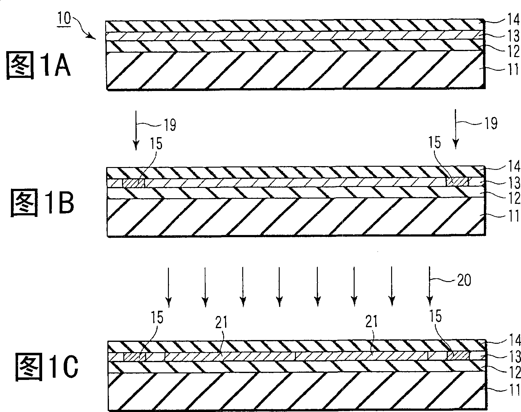
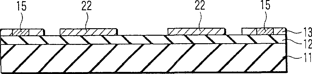
[0085] Reference will now be made to Figure 1A to Figure 1E A first embodiment of the present invention will be described. First, a support substrate 11 formed of an insulating material such as a glass substrate, a quartz substrate, or a plastic substrate is prepared. Using this supporting substrate 11 , a semiconductor film forming substrate 10 including this supporting substrate 11 and a semiconductor film 13 on this supporting substrate 11 will be manufactured. In the case where the present invention is applied to, for example, a liquid crystal display, it is recommended to use an alkali-free glass substrate such as Corning #1737 as the support substrate 11 . The material of the supporting substrate 11 in the present invention is not limited to insulating materials. A semiconductor substrate such as Si, Ge, SiGe, SiGeC, GaAs, GaP, InAs, GaN, ZnTe, CdSe, or CdTe may be used as necessary.

[0086] On this support substrate 11 is formed an insulating film 12 serving as an ...

no. 2 example

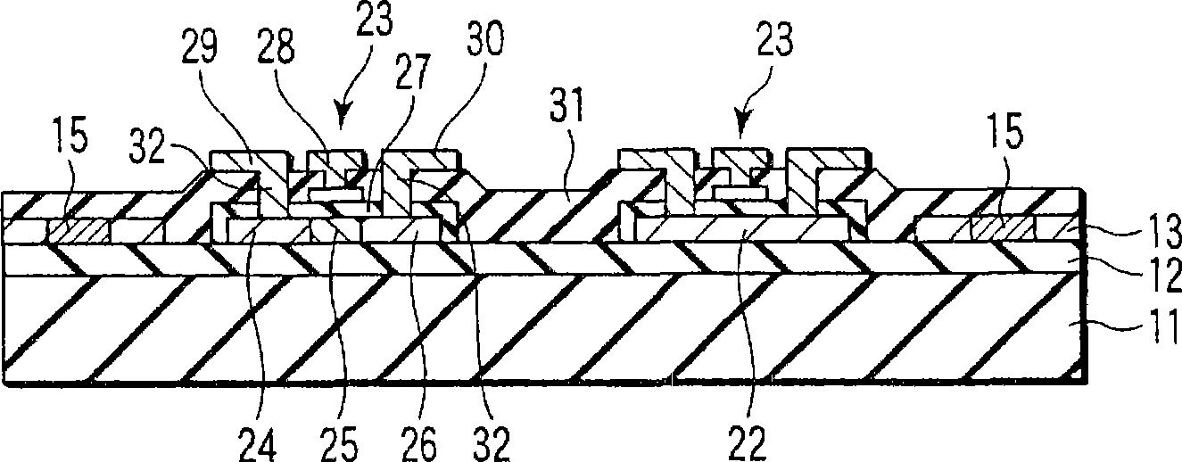
[0124] Next, the second embodiment will be described in detail. In the second embodiment, for example, as Figure 12A As shown, using the phase value modulation type mask pattern MK, an alignment mark for alignment is formed on a semiconductor film on a substrate. The techniques that will be described below are applicable to uses other than forming alignment marks.

[0125] Figure 10 An example of a crystallization apparatus suitable for forming the alignment mark in the second embodiment is schematically shown. exist Figure 10 The laser beam used in the crystallization apparatus shown has, for example, a wavelength of 248 nm for heating the non-single crystal semiconductor film formed on the substrate 206 . The crystallization device may include, for example, a KrF excimer laser 201 that can output a laser beam capable of melting the irradiated portion of the non-single crystal semiconductor film. As another example, a YAG laser may be used as a light source. Also, an...

no. 3 example

[0184] Next, an embodiment of the light transmission quantity modulation type will be described in which the mark pattern MK, such as a metal material capable of blocking light, is arranged on a glass substrate with a predetermined width (area) and pitch (interval).

[0185] Figure 18 A case where the mark pattern MK is applied to a method other than the above-described method of changing the phase value is shown. In this third implementation, alignment marks are formed on the semiconductor film on the substrate using the light-blocking type mask pattern MK. The techniques that will be described below are applicable to uses other than forming alignment marks.

[0186] In this case, a light-blocking metal film is selectively provided. Therefore, a shielding portion PS (or Pt) and a non-shielding portion (ie, light-transmitting portion) Ss (or St) having a predetermined area per 1 block (1 cell) are provided. For example, if Figures 19A to 19C As shown, in each 1 zone (1 u...


PUM

PropertyMeasurementUnit
widthaaaaaaaaaa
refractive indexaaaaaaaaaa

Abstract

Exact alignment of a recrystallized region, which is to be formed in an amorphous or polycrystalline film, is facilitated. An alignment mark is formed, which is usable in a step of forming an electronic device, such as a thin-film transistor, in the recrystallized region. In addition, in a step of obtaining a large-grain-sized crystal-phase semiconductor from a semiconductor film, a mark structure that is usable as an alignment mark in a subsequent step is formed on the semiconductor film in the same exposure step. Thus, the invention includes a light intensity modulation structure that modulates light and forms a light intensity distribution for crystallization, and a mark forming structure that modulates light and forms a light intensity distribution including a pattern with a predetermined shape, and also forms a mark indicative of a predetermined position on a crystallized region.

Description

[0001] This application is a divisional application. The original application was a patent application submitted to the China Patent Office on August 9, 2005. The application number is 200510091162.1, and the title of the invention is "semiconductor device including a semiconductor thin film, crystallization method and device for the thin film" . Background of the invention [0002] The present invention relates to a crystallization method of a semiconductor thin film, a substrate having a crystallized semiconductor thin film, a crystallization device for a semiconductor thin film, an optical modulation element used in the crystallization device, a semiconductor device formed in a crystallized thin film, and a thin film semiconductor device Manufacturing methods, all of which are applicable to electronic devices such as active matrix flat panel displays. Specifically, the present invention relates to a technique of forming an alignment mark for alignment in the case where a re...

Claims


Application Information

Patent Timeline
Patent Type & Authority Applications(China)
IPC IPC(8): G02F1/015G02F1/01H01L21/268H01L21/77H01L23/544H01L27/12H01L29/786
Inventor 小川裕之秋田典孝谷口幸夫平松雅人十文字正之松村正清
Owner LG ELECTRONICS INC
Why Eureka
Try Eureka