Structure for packing bearing belt and method of manufacturing the same

A manufacturing method and technology for carrying tapes, which are applied in semiconductor/solid-state device manufacturing, semiconductor/solid-state device components, semiconductor devices, etc., and can solve problems such as large rebound force, decreased process yield, and fracture.

Inactive Publication Date: 2009-05-27
CHIPMOS TECH INC
View PDF0 Cites 0 Cited by
  • Summary
  • Abstract
  • Description
  • Claims
  • Application Information

AI Technical Summary

Problems solved by technology

In this known method, the pressurization stroke of the inner pin area 121 is longer, and the bending deformation of the inner pin area 121 formed during pressing will generate a relatively large resilience force, which will cause the problem of poor bonding.
The inner lead area 121 is also prone to breakage at the bent

Method used


Image

  • Structure for packing bearing belt and method of manufacturing the same
  • Structure for packing bearing belt and method of manufacturing the same
  • Structure for packing bearing belt and method of manufacturing the same

Examples


Embodiment Construction

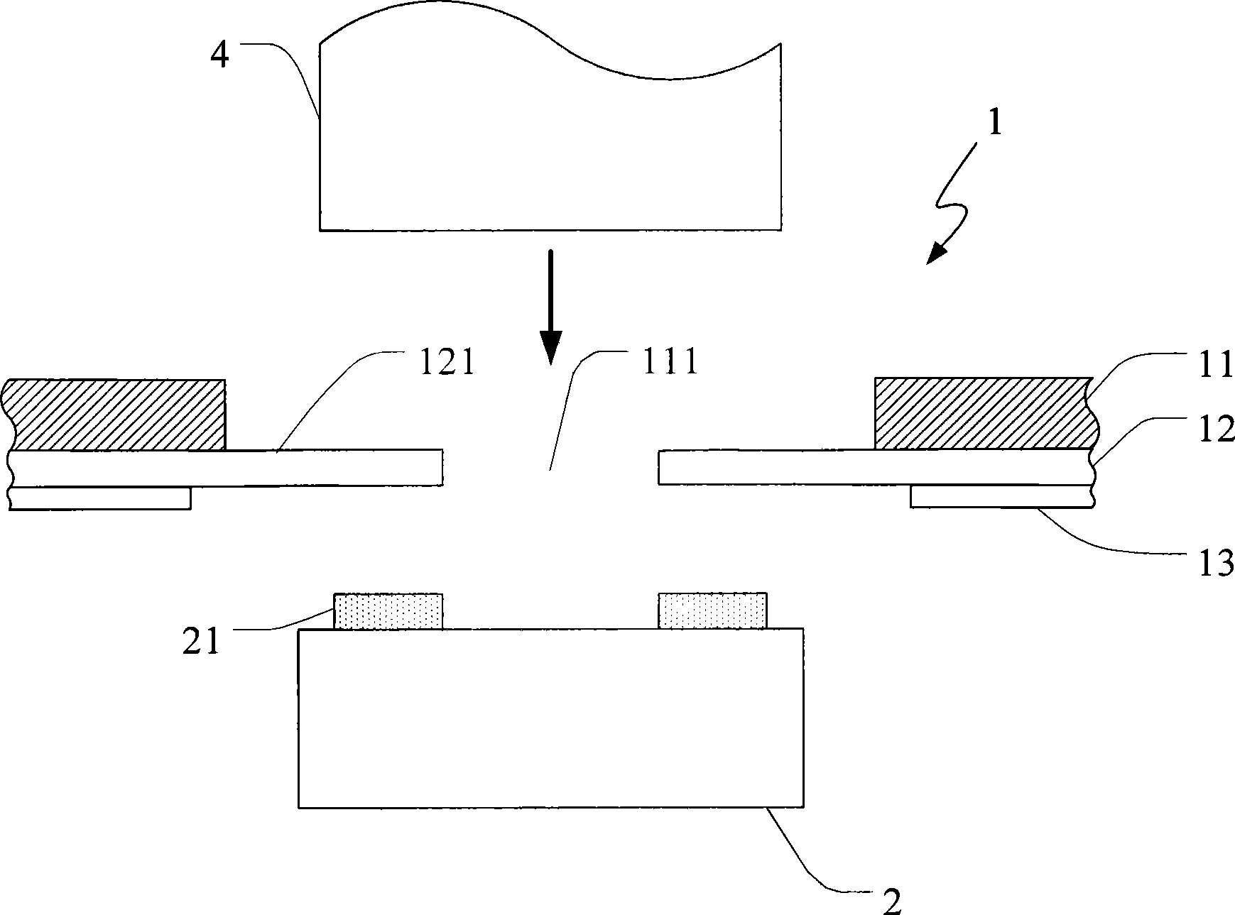
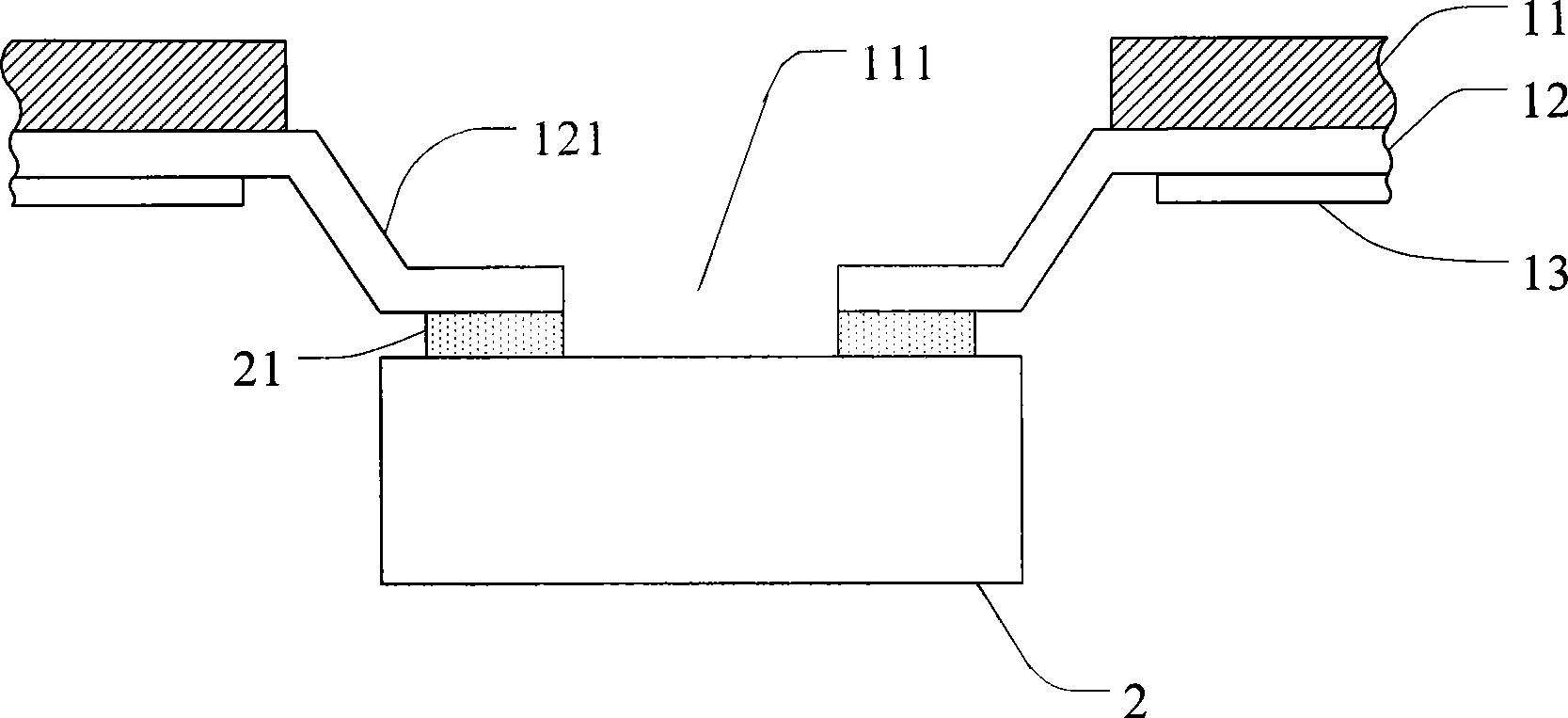
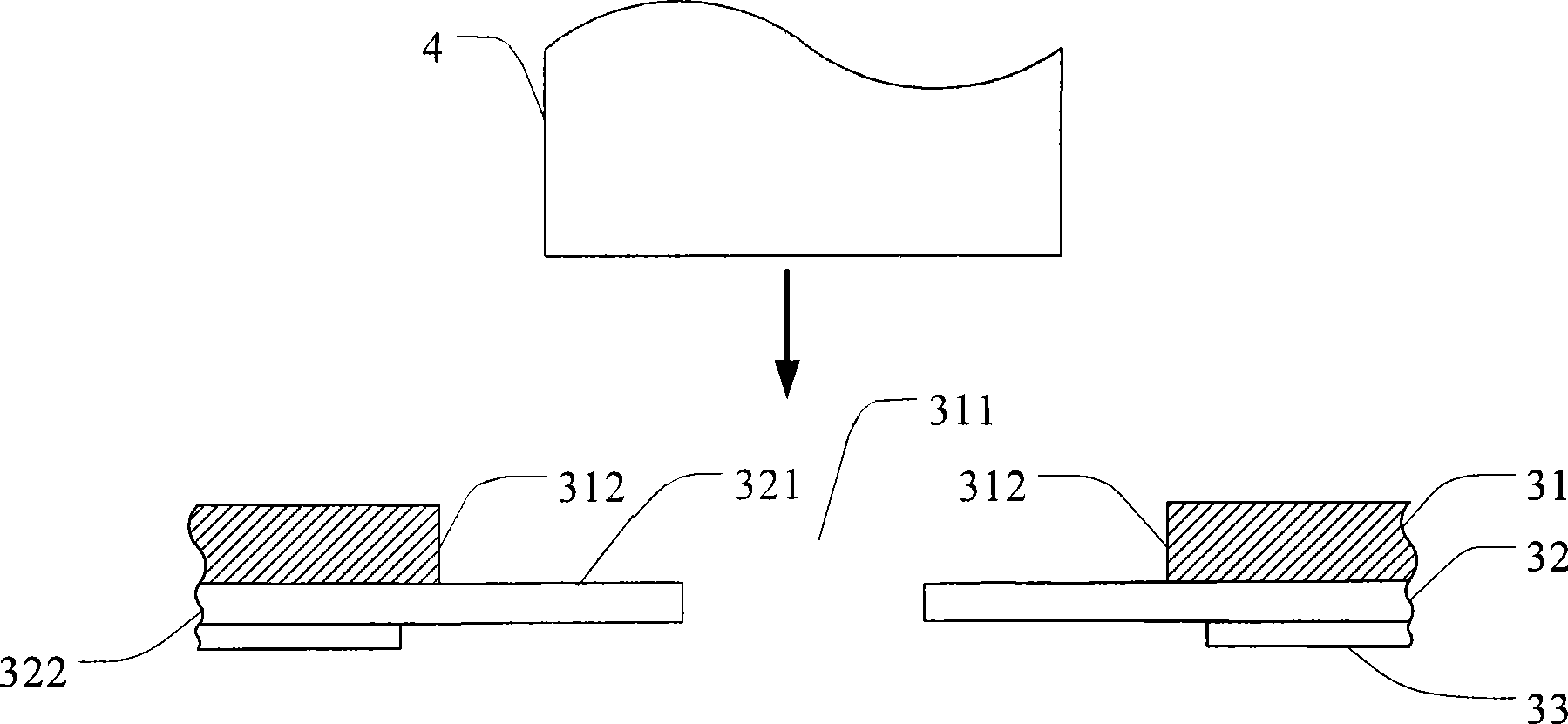
[0028] Please refer to the structure of the package carrier tape 3 disclosed in an embodiment of the present invention Figure 2B , including a flexible substrate layer 31 , a lead layer 32 , and a part of the solder resist layer 33 covering the lead layer 32 . The flexible base material layer 31 is formed with a through hole 311 defined by an edge 312 on the flexible base material layer 31 . For the convenience of illustration, the wiring layer 32 can be divided into different areas, including the first lead area 321 and the second lead area 322. As shown in the figure, the second lead area 322 is formed on the flexible substrate layer 31, And the solder resist layer 33 partially covers the second lead area 322 , and the first lead area 321 extends from the peripheral edge 312 toward the through hole 311 . The feature of this embodiment is that the first lead area 321 is pre-shaped as a bent portion away from the flexible base material layer 31, preferably, the bent portion ...


PUM


Abstract

The invention relates to a structure for an encapsulation bearing belt and a manufacture method thereof. Before the encapsulation bearing belt is jointed with a chip, a pin of the encapsulation bearing belt on a through hole forms a bending part, so that when the encapsulation bearing belt is in encapsulation joint with the chip subsequently, the pin can not be easily deflected, cracked or stripped, further the process yield of jointing the chip to the encapsulation bearing belt can be greatly improved, and cost for manufacturing the encapsulation bearing belt is saved.

Description

technical field [0001] The present invention relates to a structure of a packaging carrier tape and a manufacturing method thereof; in particular, a structure and a manufacturing method of a packaging carrier tape used for a tape carrier package (Tape Carrier Package, TCP). Background technique [0002] With the advancement of industry, various liquid crystal screens and electronic products with folding functions have been widely used in daily life. Among them, because the flexible circuit board has the advantages of thin thickness, small pin spacing, and high number of pins, when the LCD screen is used to save space, or the electronic product is used to achieve the folding function, the flexible circuit board becomes a Indispensable component. [0003] Generally speaking, a semiconductor chip is packaged on the flexible circuit board and electrically connected with other external components. With the evolution of packaging technology, the ways of chip packaging on flexibl...

Claims


Application Information

Patent Timeline
IPC IPC(8): H01L23/498H01L21/48
CPCH01L24/50H01L2224/50H01L2924/00012
Inventor 刘宏信沈弘哲李世富萧世鑫
Owner CHIPMOS TECH INC
Why Eureka
Try Eureka