Thin-film transistor array substrate and patching method thereof

A thin-film transistor and array substrate technology, applied in the field of liquid crystal display, can solve problems such as light leakage that cannot be solved

Active Publication Date: 2009-05-27
KUSN INFOVISION OPTOELECTRONICS
View PDF0 Cites 20 Cited by
  • Summary
  • Abstract
  • Description
  • Claims
  • Application Information

AI Technical Summary

Problems solved by technology

Due to the limitation of the low voltage Vgl on the gate line and the inability to change the common voltage signal Vcom, the voltage across the repaired liquid crystal capacitor cannot be adjusted to

Method used


Image

  • Thin-film transistor array substrate and patching method thereof
  • Thin-film transistor array substrate and patching method thereof
  • Thin-film transistor array substrate and patching method thereof

Examples


Embodiment Construction

[0026] In order to make the object, technical solution, and advantages of the present invention clearer, the present invention will be further described in detail below with reference to the accompanying drawings and examples.

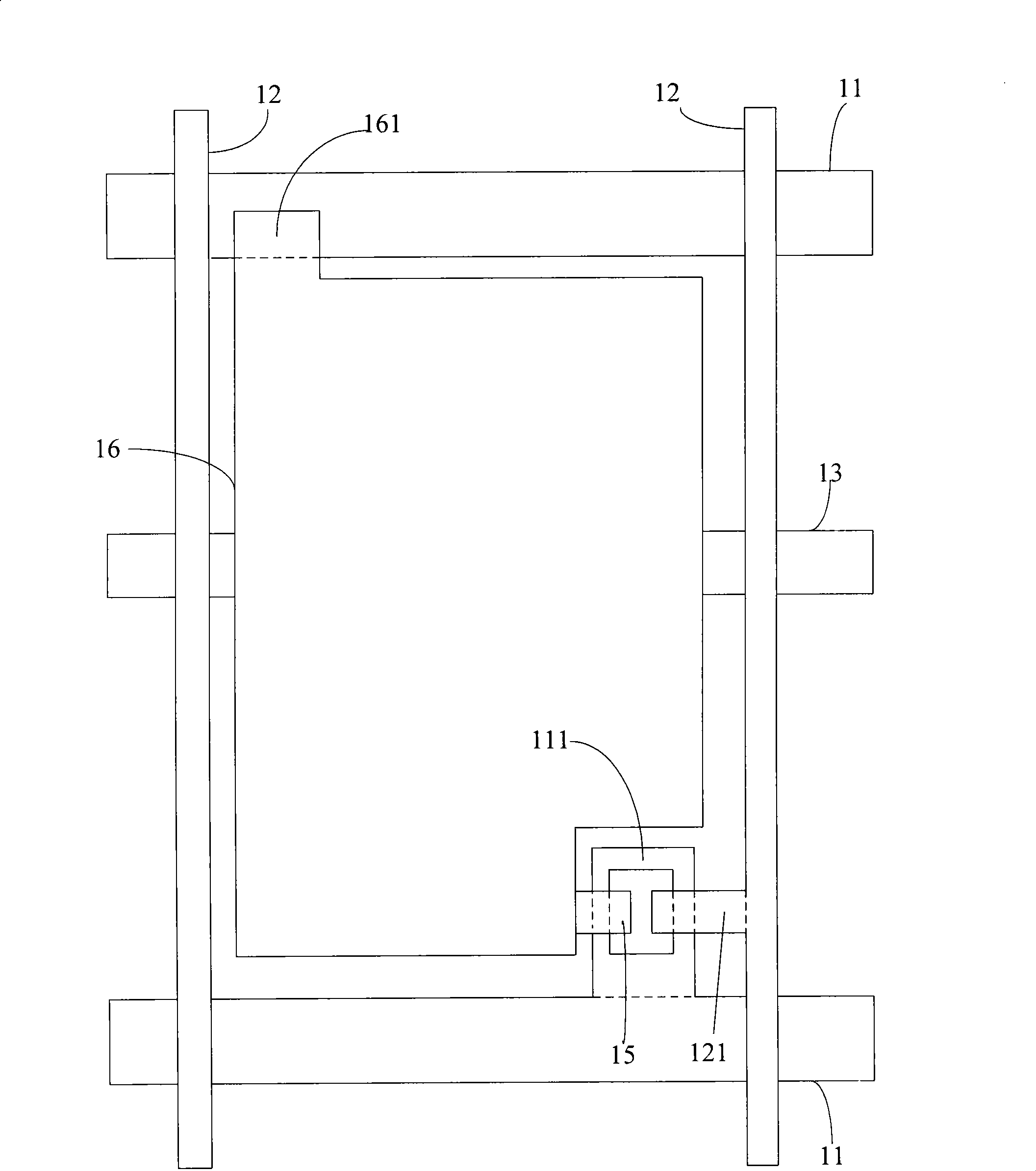
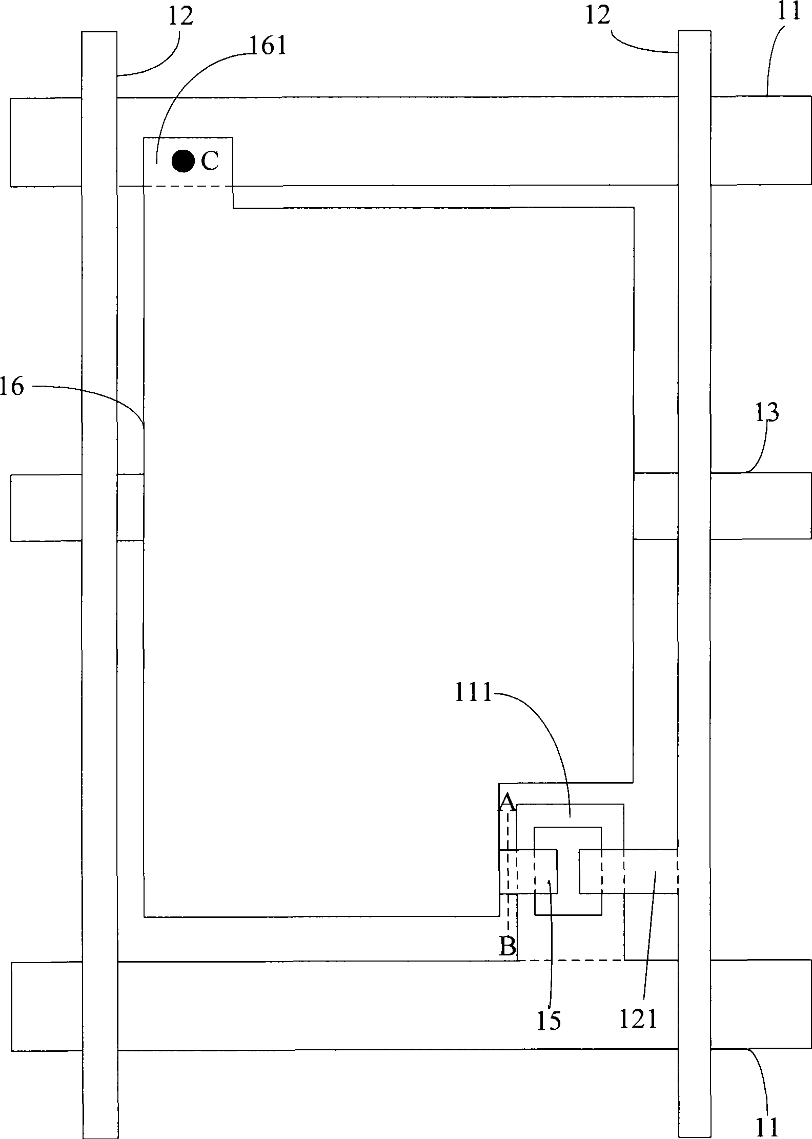
[0027] The liquid crystal display of the embodiment of the present invention includes a liquid crystal panel, and the liquid crystal panel includes a thin film transistor array substrate, a color filter substrate and a liquid crystal layer filled between the two substrates. For clarity of illustration, no color filter substrate is drawn in the drawings of the embodiments of the present invention. Figure 4 It is a schematic structural diagram of a single pixel in the thin film transistor array substrate of the present invention. The gate lines 11 and the data lines 12 are vertically insulated and cross-arranged on the base substrate ( Figure 4 (not shown in ), thereby defining a pixel area in which a pixel electrode 16 is formed. A thin film transis...


PUM


Abstract

The invention provides a thin film transistor array substrate. The key points of the invention comprise that a pixel region is also provided with a first element and a second element; the first element comprises a grid insulation layer directly covering the surface of a substrate base plate, a semiconductor layer formed on the grid insulation layer and a first source electrode and a first drain electrode which are both formed on the semiconductor layer; and the second element comprises a grid insulation layer directly covering the surface of the substrate base plate, a semiconductor layer formed on the grid insulating layer and a second source electrode and a second drain electrode which are both formed on the semiconductor layer. For the thin film transistor array substrate with a pixel repairing structure, when the pixel bright spot defect generates, by utilizing a repairing method for the thin film transistor array substrate provided by the invention, the voltage at both ends of a liquid crystal capacitor is approach to the voltage difference VL0 corresponding to the darkest gray scale L0 in the end, so no light leakage occurs while viewing from different visual angles.

Description

technical field [0001] The invention relates to the technical field of liquid crystal display, in particular to a thin film transistor array substrate with a pixel repair structure and a repair method thereof. Background technique [0002] At present, liquid crystal display, as a kind of flat panel display, has been widely used in various fields, and it has the advantages of low power consumption, thin shape and light weight. Generally, a liquid crystal display includes a liquid crystal panel, which includes a TFT array substrate with pixel electrodes, a color filter substrate with common electrodes, and a liquid crystal layer filled between the TFT array substrate and the color filter substrate. An electric field is generated between the pixel electrode and the common electrode, and the intensity of the electric field applied to the liquid crystal layer is controlled by the two electrodes to control the transmittance of incident light, thereby realizing the control of brigh...

Claims


Application Information

Patent Timeline
IPC IPC(8): H01L27/12H01L21/768G02F1/1362G02F1/13
Inventor 钟德镇廖家德
Owner KUSN INFOVISION OPTOELECTRONICS
Why Eureka
Try Eureka