Magneto-resistive effect device of the cpp type, and magnetic disk system

A magneto-resistance effect element and magneto-resistance effect technology, applied to electrical components, measuring devices, and resistors controlled by a magnetic field, can solve problems such as characteristic changes, unstable pinning functions, and insufficient pinning functions

Inactive Publication Date: 2009-06-03
TDK CORPARATION
View PDF6 Cites 8 Cited by
  • Summary
  • Abstract
  • Description
  • Claims
  • Application Information

AI Technical Summary

Problems solved by technology

However, in the proposed structure, each antiferromagnetic material layer needs to have a thickness of more than 5nm in order to realize the practical effect, which can be said to be inconsistent with the purpose of reducing the "read gap length".
Furthermore, there is a problem that it is necessary to make the direction of the exchange coupling between the two antiferromagnetic material layers opposi

Method used


Image

  • Magneto-resistive effect device of the cpp type, and magnetic disk system
  • Magneto-resistive effect device of the cpp type, and magnetic disk system
  • Magneto-resistive effect device of the cpp type, and magnetic disk system

Examples


experiment example 1

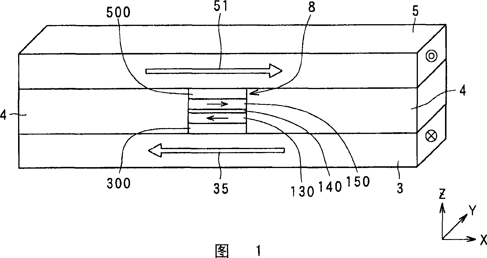
[0197] production including Figure 1 and figure 2 An experimental sample (sample of Example 1) of a magnetoresistance effect element having the structure shown.

[0198] That is, as shown in Table 1 below, on the first shield layer 3 made of NiFe with a width of 30 μm (dimensions in the X-axis direction), a length of 3 μm (dimensions in the Y-axis direction), and a thickness of 100 nm (dimensions in the Z-axis direction), A magnetoresistance effect portion 8 having a stacked structure shown in Table 1 was formed, and on this magnetoresistance effect portion 8, a width of 30 μm (dimension in the X-axis direction), a length of 3 μm (dimension in the Y-axis direction), and a thickness of 100 nm (Z The second shielding layer 5 made of NiFe. Both sides of the magnetoresistance effect part 8 are insulated by alumina.

[0199] The first shielding layer 3 and the second shielding layer 5 respectively utilize the shape anisotropy caused by the above-mentioned dimensions to form a si...

experiment example 2

[0205] In the experimental example 1 sample of the above-mentioned experimental example 1, the material of the nonmagnetic intermediate layer 140 constituting the sensor region was changed from a three-layer laminated body of Cu (thickness 0.5 nm) / ZnO (thickness 1.8 nm) / Cu (thickness 0.5 nm) Change to MgO (thickness 0.8nm).

[0206] Except for this, an experimental sample (sample of Example 2) of a magnetoresistance effect element was produced in the same manner as in Example 1 above.

[0207] Using the magnetoresistance effect of the sample of Example 2 formed in this way, a signal magnetic field from a medium corresponding to -400Oe to 400Oe was detected, and it was confirmed that a practical magnetoresistance change was obtained.

experiment example 3

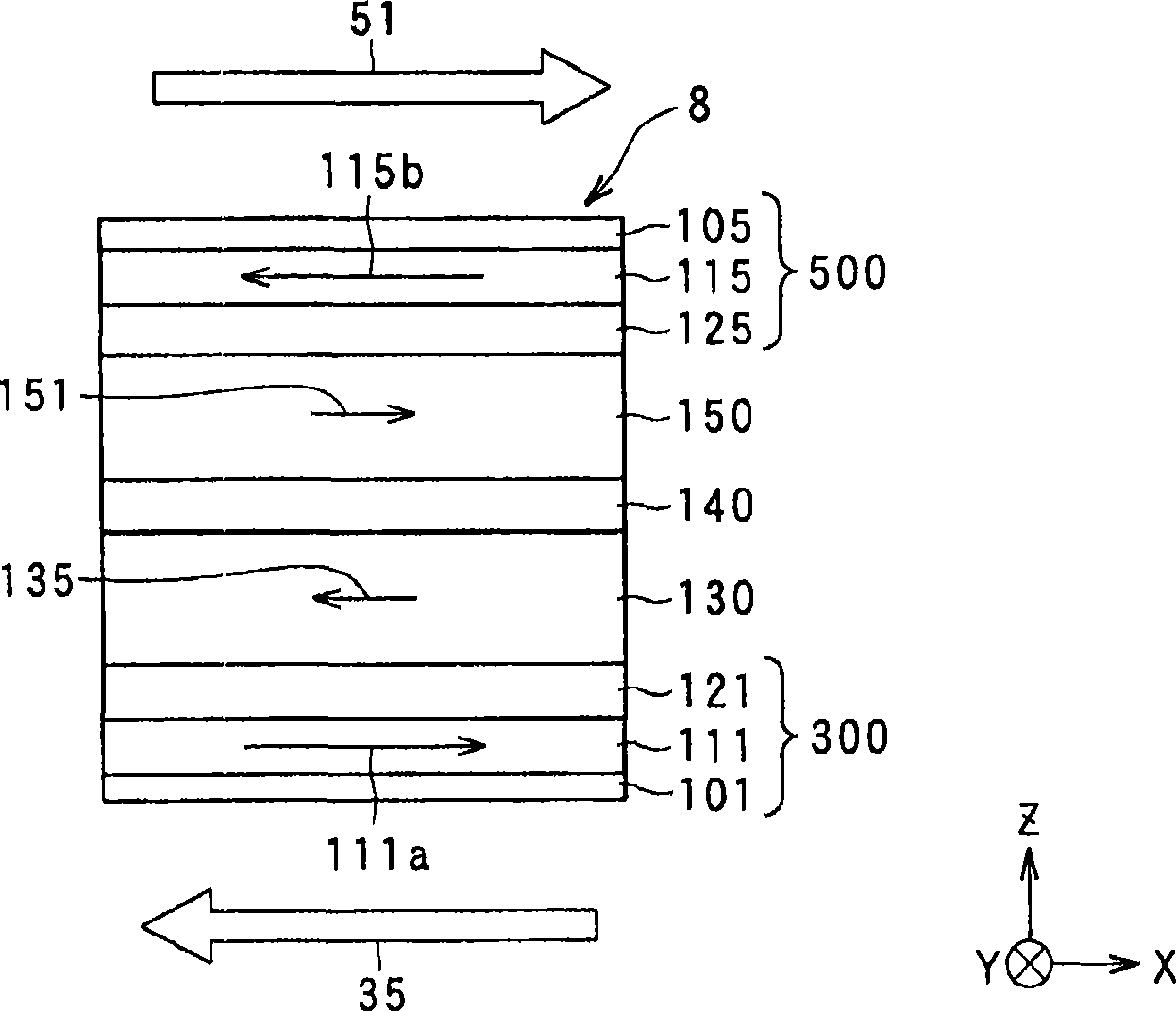
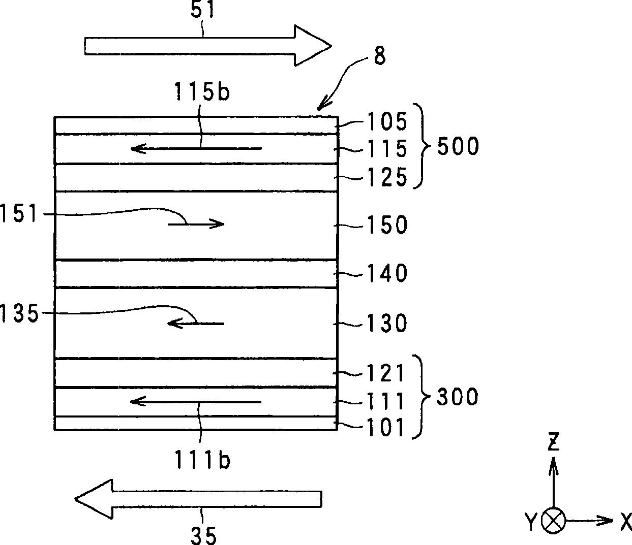
[0209] In the example 1 sample of the above-mentioned experimental example 1, the lamination structure of the first exchange coupling gap layer 300 and the second exchange coupling gap layer 500 was changed to the mode shown in the following Table 2 to produce Figure 10 Experimental sample (sample of Example 3) of the magnetoresistance effect element of the embodiment shown.

[0210] In the structure shown in Table 2, like Figure 10 As shown, the magnetization 35 of the first shielding layer 3 is antiferromagnetically coupled to the magnetization 111a of the gap adjustment layer 111, the magnetization 111a of the gap adjustment layer 111 is antiferromagnetically coupled to the magnetization 112b of the gap adjustment layer 112, and the magnetization 112b of the gap adjustment layer 112 is antiferromagnetically coupled. The magnetization 112b is antiferromagnetically coupled to the magnetization 135 of the first ferromagnetic layer 130 . Similarly, the magnetization 51 of th...


PUM


Abstract

The invention provides a magneto-resistive effect device of a CPP (current perpendicular to plane) structure, comprising a magneto-resistive effect unit, and a first shield layer and a second shield layer located and formed such that the magneto-resistive effect unit is sandwiched between them, with a sense current applied in a stacking direction, characterized in that: said magneto-resistive effect unit comprises a non-magnetic intermediate layer, and a first ferromagnetic layer and a second ferromagnetic layer stacked and formed such that said nonmagnetic intermediate layer is interposed between them, wherein: said first shield layer, and said second shield layer is controlled by magnetization direction control means in terms of magnetization direction, and said first ferromagnetic layer, and said second ferromagnetic layer receives action such that there is an antiparallel magnetization state created, in which mutual magnetizations are in opposite directions, under influences of magnetic actions of said first shield layer and said second shield layer. It is thus possible to achieve an antiparallel magnetization state for two ferromagnetic layers with simple structure yet without being restricted by the material and specific structure of an intermediate film interposed between the two ferromagnetic layers.

Description

technical field [0001] The present invention relates to a magnetoresistance effect element for reading the magnetic field intensity of a magnetic recording medium etc. as a signal, a thin film magnetic head provided with the magnetoresistance effect element, and a head gimbal assembly (head gimbal assembly) including the thin film magnetic head and disk device. Background technique [0002] In recent years, along with the increase in recording density of hard disks (HDDs), performance improvements in thin-film magnetic heads have also been demanded. As a thin-film magnetic head, a composite thin-film magnetic head is widely used, which is a reproduction head with a read-only magnetoresistance effect element (hereinafter sometimes abbreviated as MR (Magneto-resistive: magnetoresistive) element) and a write-only induction head. The structure of the recording head of the type magnetic conversion element. [0003] At present, magnetoresistance effect elements (CIP-GMR elements...

Claims


Application Information

Patent Timeline
IPC IPC(8): H01L43/08H01F10/32G11B5/39G11B5/31
CPCB82Y10/00B82Y25/00G11B5/3909H01L43/08G11B5/3912H01F10/3254G11B2005/3996G01R33/098H01F10/30
Inventor 岛泽幸司宫内大助土屋芳弘町田贵彦原晋治
Owner TDK CORPARATION
Why Eureka
Try Eureka