Printed circuit board test system and test method

A technology for printed circuit boards and test systems, which is applied to electronic circuit testing, components of electrical measuring instruments, and electrical measurement, etc., can solve problems such as inconvenience in actual use and the inability to reuse test fixtures, so as to reduce production and testing costs, achieve the effect of reuse

Inactive Publication Date: 2009-06-17
KONKA GROUP
View PDF0 Cites 17 Cited by
  • Summary
  • Abstract
  • Description
  • Claims
  • Application Information

AI Technical Summary

Problems solved by technology

This technology has the following defects: the test fixture cannot be reused
[0004] In summary, the existing PCB board testing technology scheme obviously has inconvenience and defects in actual use, so it is necessary to improve it

Method used


Image

  • Printed circuit board test system and test method
  • Printed circuit board test system and test method
  • Printed circuit board test system and test method

Examples


Embodiment Construction

[0032] In order to make the object, technical solution and advantages of the present invention clearer, the present invention will be further described in detail below in conjunction with the accompanying drawings and embodiments. It should be understood that the specific embodiments described here are only used to explain the present invention, not to limit the present invention.
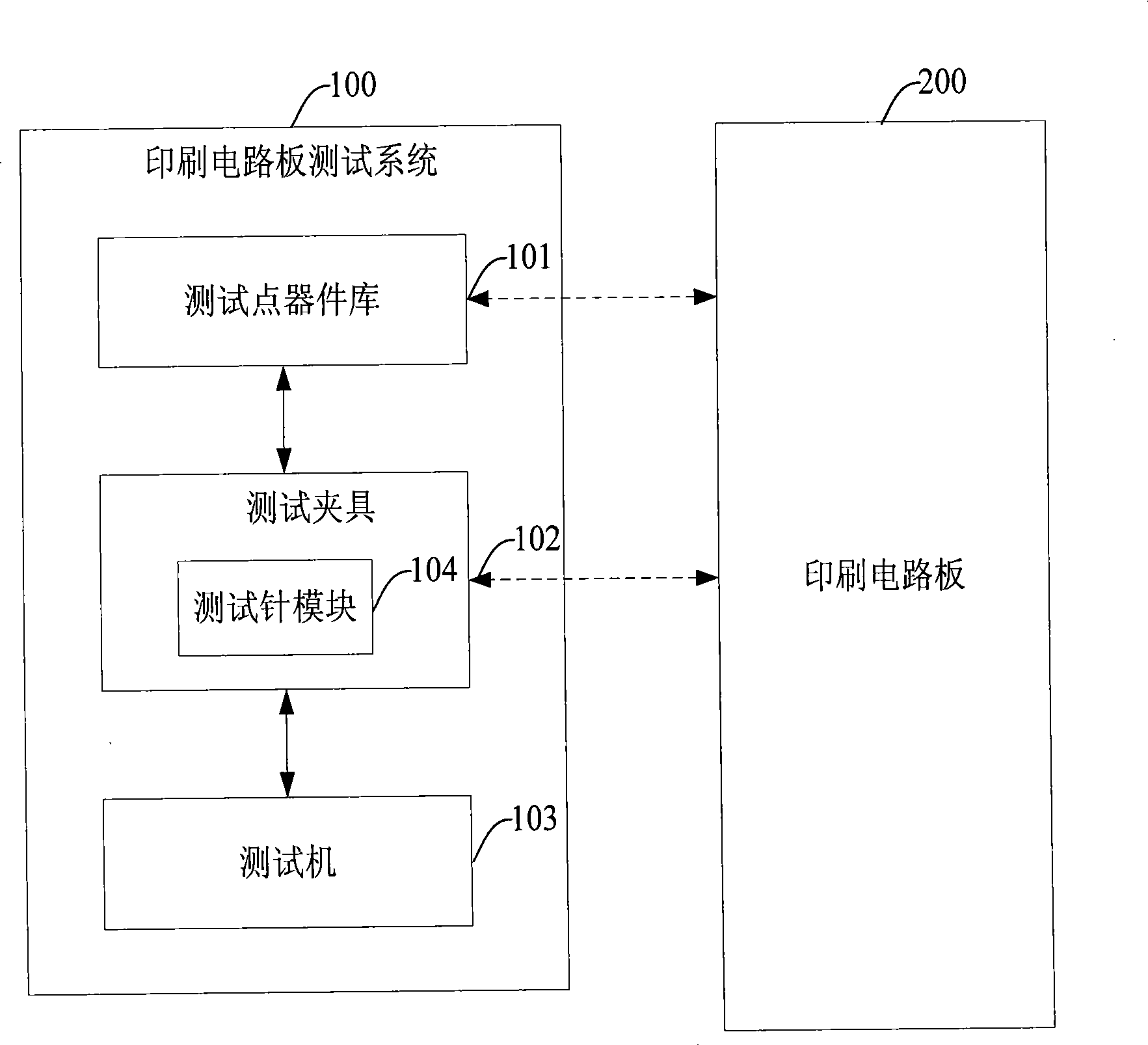
[0033] The basic idea of ​​the present invention is to arrange a plurality of test points into a common shape to form a test point device, store the test point device in the test point device library, and select the test point from the test point device library during the production process of the printed circuit board The device is then positioned on the printed circuit board by the test fixture on the test point device selected by the printed circuit board, and finally the testing machine tests the positioned test point device.

[0034] The printed circuit board testing system 100 provided by the...


PUM


Abstract

The invention discloses a printed circuit board test system, which comprises a test point component library, a test fixture and a test machine; wherein, the test point component library is used for storing a plurality of test point components for clicking the printed circuit boards; the test fixture is used for positioning the test point components clicking the printed circuit board on the printed circuit board; the test machine is used for testing the positioned test point components on the printed circuit board. The invention correspondingly discloses a printed circuit board test method. Therefore, the system realizes the repeated use of the test fixture and reduces the production and test costs.

Description

technical field [0001] The invention relates to the technical field of electronic circuit testing, in particular to a PCB (Printed Circuit Board, printed circuit board) testing system and testing method. Background technique [0002] PCB board (Printed Circuit Board, printed circuit board) is one of the important components of the electronics industry. It can provide mechanical support for the fixing and assembly of various electronic components such as integrated circuits, realize the wiring and electrical connection or electrical insulation between various electronic components such as integrated circuits, and provide the required electrical characteristics, such as characteristic impedance, etc. Provide solder mask graphics for automatic soldering and provide identification characters and graphics for component insertion, inspection, and maintenance. Now almost every kind of electronic equipment, such as electronic watches, calculators, computers, communication electroni...

Claims


Application Information

Patent Timeline
Patent Type & Authority Applications(China)
IPC IPC(8): G01R31/28G01R1/073
Inventor 易耀师
Owner KONKA GROUP
Why Eureka
Try Eureka