Method for cleaning wafer surface pollutant particle in CMP process

A contaminant, wafer technology, applied in electrical components, semiconductor/solid-state device manufacturing, circuits, etc., can solve problems such as inaccurate display of machine working conditions, too large differences, etc., to achieve moderate speed and selection ratio, use Safe, convenient and cost-effective

Inactive Publication Date: 2009-06-17
SEMICON MFG INT (SHANGHAI) CORP
View PDF1 Cites 9 Cited by
  • Summary
  • Abstract
  • Description
  • Claims
  • Application Information

AI Technical Summary

Problems solved by technology

[0007] After using the chemical mechanical polishing method of the prior art to polish the control sheet and the dummy sheet and cleaning the control sheet and the dummy sheet with the cleaning method of the prior art, it was found that the surface size of the control sheet and the dummy sheet was larger than 0.16um. The number is still relatively large, usually greater than 100. The surface cleanliness of this cleanliness control sheet and virtual sheet is too different from the cleanliness of the online wafer surface, which cannot accurately display the actual working status of the machine. When the device size is getting smaller and smaller and the process requirements are getting stricter, it is not allowed

Method used


Image

  • Method for cleaning wafer surface pollutant particle in CMP process
  • Method for cleaning wafer surface pollutant particle in CMP process
  • Method for cleaning wafer surface pollutant particle in CMP process

Examples


Embodiment

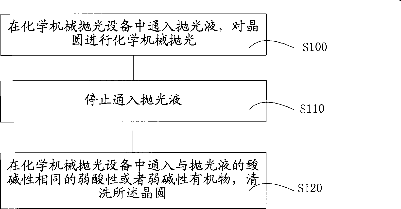
[0026] A method for removing pollutant particles on the wafer surface in a CMP process, referring to the appended figure 1 , including: S100, injecting polishing fluid into the chemical mechanical polishing equipment, and performing chemical mechanical polishing on the wafer; S110, stopping injecting the polishing fluid; S120, injecting the same acidity and alkalinity as the polishing fluid into the chemical mechanical polishing equipment Weakly acidic or weakly alkaline organic matter to clean the wafer.

[0027] The wafer described in this embodiment is a blank semiconductor wafer or a control sheet or a dummy sheet with a film layer on the surface, or a wafer with some film layers or devices formed on the surface during the manufacturing process of the semiconductor device.

[0028] Wherein, the film layers mentioned on the wafer surface refer to all film layers in the manufacturing process of semiconductor devices, such as insulating materials such as silicon oxide and sil...


PUM


Abstract

Disclosed is a method for clearing pollutant particles on surfaces of a wafer in the CMP technique, the steps of the method comprise leading polishing solution in a chemical mechanical polishing device to perform chemical mechanical polishing on the wafer, stopping leading in the polishing solution, putting acidulous or alkalescent organic substances of which acidity or alkaline is identical to the polishing solution in the chemical mechanical polishing device, and then cleaning the wafer. The method can efficiently remove large-size pollutant particles on the surfaces of the wafer which can not be cleaned after mechanically polishing the wafer in the prior art.

Description

technical field [0001] The invention relates to the technical field of semiconductor manufacturing, in particular to a method for removing pollutant particles on the wafer surface in a CMP process. Background technique [0002] With the continuous development of the semiconductor industry, the semiconductor manufacturing process has entered the nanometer era. In order to adapt to the trend of smaller and smaller electronic products and stronger functions, the line width in the semiconductor manufacturing process has also been developed from the original 0.18 micron to the present. 0.13 micron or even 90nm process. Along with the trend of chip functions becoming stronger and stronger, and components becoming smaller and smaller, the quality requirements for the surface of semiconductor wafers are also getting higher and higher, and the surface of the wafer is required to be flat and smooth, free of pollutant particles clean surface. The pollutant particles refer to various ...

Claims


Application Information

Patent Timeline
Patent Type & Authority Applications(China)
IPC IPC(8): H01L21/00H01L21/02H01L21/302H01L21/304H01L21/306
Inventor 张斐尧杜应提周静
Owner SEMICON MFG INT (SHANGHAI) CORP
Why Eureka
Try Eureka