Method for forming light-transmitting regions and image sensing apparatus

A technology for image sensing devices and light-transmitting regions, which is applied in radiation control devices, semiconductor devices, electrical components, etc., can solve problems such as long manufacturing time, inconsistent exposure consistency and reproducibility, high manufacturing cost of photolithography technology, etc. To achieve the effect of saving manufacturing cost and time

A technology for image sensing devices and light-transmitting regions, which is applied in radiation control devices, semiconductor devices, electrical components, etc., can solve problems such as long manufacturing time, inconsistent exposure consistency and reproducibility, high manufacturing cost of photolithography technology, etc. To achieve the effect of saving manufacturing cost and time

CN101465320AActive Publication Date: 2009-06-24VISERA TECH CO LTD +1

Image

  • Method for forming light-transmitting regions and image sensing apparatus
  • Method for forming light-transmitting regions and image sensing apparatus
  • Method for forming light-transmitting regions and image sensing apparatus

Examples


Embodiment Construction

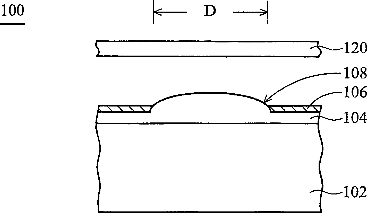
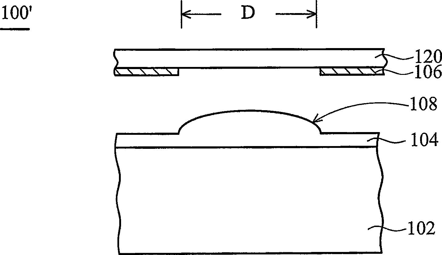
[0047] figure 1 and figure 2 It is a series of cross-sectional schematic diagrams, respectively partially showing image sensing devices according to different embodiments of the present invention.

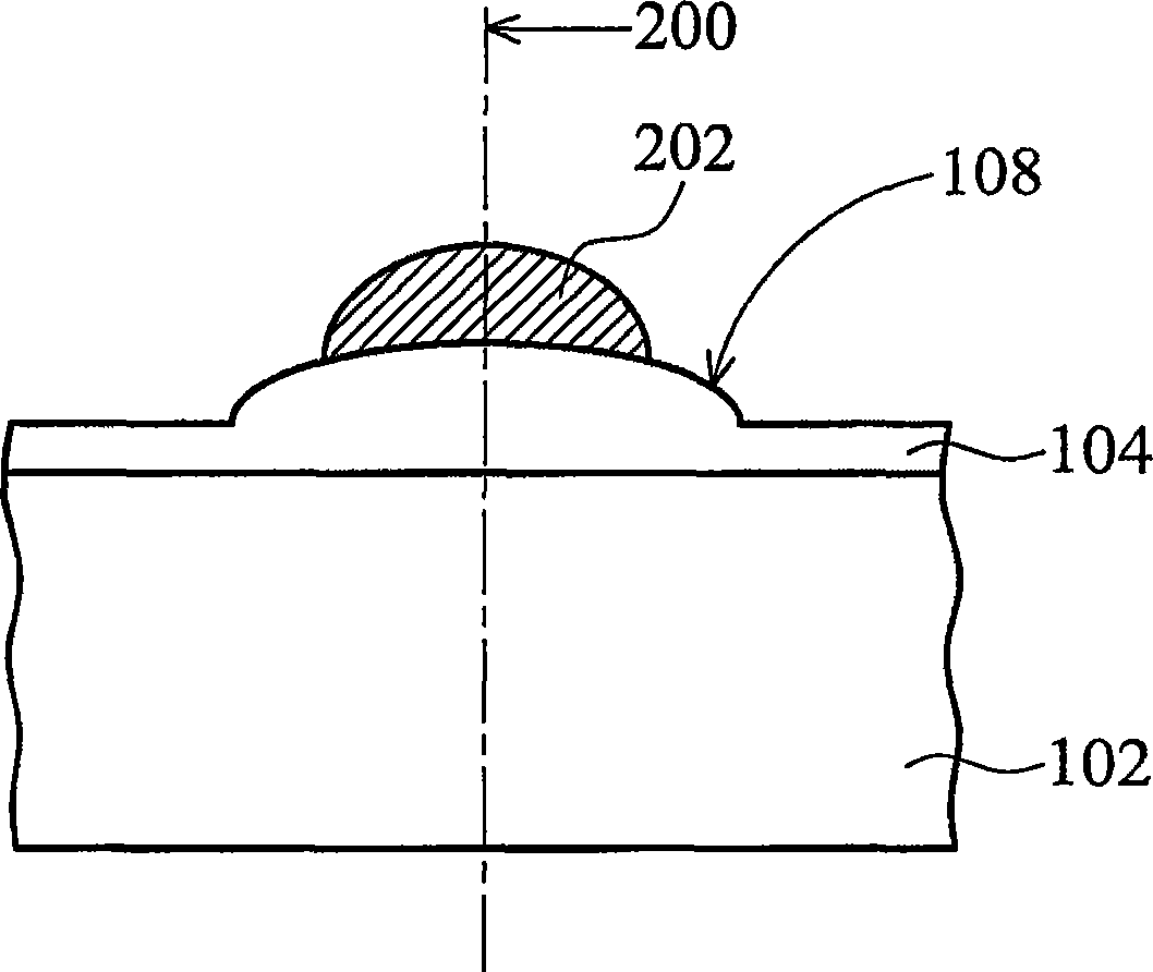
[0048] Please refer to figure 1 , which shows an image sensing device 100 , which includes an image sensing structure 102 , a microlens 104 , a light-shielding layer 106 and a light-transmitting substrate 120 . exist figure 1 The image sensing structure 102 is shown here as a planar structure, but the image sensing structure 102 may include an image sensor such as a charge-coupled device image sensor, a complementary metal-oxide semiconductor image sensor, or other types of image sensors. not shown), including a color filter layer (not shown) of a plurality of different color filters such as red, green or blue, a plurality of interconnected metal layers (not shown) and for insulating the above-mentioned interconnected Functional components such as multiple inter-metal dielectr...


PUM


Abstract

Disclosed is method for forming light-transmitting region and image sensing apparatus. A method for forming a light-transmitting region comprises: providing a support feature; forming a sacrificial layer over a portion of the support feature, wherein the sacrificial layer comprises an energy-induced swelling material; forming a light-blocking layer conformably over the support feature to cover the sacrificial layer and the support feature; subjecting the support feature, the sacrificial layer, and the light-blocking layer to an energy source to swell the sacrificial layer until bursting to thereby delaminate a portion of the light-blocking layer from the support feature and leave a light-transmitting region exposed with a portion of the support feature in the light-blocking layer. Applying a gas flow or scrub cleaning force to clean up the light-transmitting region and a top surface of the light-blocking layer remains over the support feature. The invention can save manufacturing cost and time.

Description

technical field [0001] The invention relates to the manufacture of an image sensing device, and in particular to a method for forming a light-transmitting area in the image sensing device. Background technique [0002] In recent years, image sensing devices such as solid state image sensing devices have been widely used in optoelectronic devices such as digital cameras, mobile phones and toys. Conventional image sensing devices include image sensors such as charge coupled device (CCD) image sensors and complementary metal oxide semiconductor (complementary metal oxide semiconductor, CMOS) image sensors. [0003] In solid-state image sensing devices, microlenses are usually provided to improve image sensitivity. In addition, an aperture (diaphragm) is usually provided in the solid-state image sensor device for filtering the light path of the microlens, thereby adjusting the amount of light passing through the microlens and heading toward the image sensor. [0004] The apert...

Claims


Application Information

Patent Timeline
24 Jun 2009
Publication
CN101465320A
IPC
H01L21/82; H01L27/146; H01L27/148
CPC
H01L27/14623; H01L27/14685; H01L27/14627; H01L27/14818
Inventors
郑杰元; 林孜翰