Semiconductor encapsulation conformation and used substrate thereof

A technology for semiconductors and substrates, which is applied in the field of window-type semiconductor packaging structures and substrates. It can solve the problems of general products without structure, mold flow is not easy to fill the surrounding small windows, and the shape of holes is difficult.

Inactive Publication Date: 2009-07-01
POWERTECH TECHNOLOGY
View PDF0 Cites 2 Cited by
  • Summary
  • Abstract
  • Description
  • Claims
  • Application Information

AI Technical Summary

Problems solved by technology

Since the shape of the peripheral small windows 113 is square or rectangular, and its size is much smaller than the central slot 117, the side structure of the substrate 110 will not be weakened excessively, but a large number of peripherals are required in manufacturing. The small window 113 not only makes the hole shape difficult, but also increases the manufacturing cost of the substrate
In addition, the mold flow forming the molding compound 140 is not easy to fill the peripheral small windows 113, and there is a problem of mold overflow
[0005] It can be seen that the above-mentioned existing semiconductor packaging structure and the substrate used therein obviously still have inconvenience and defects in structure and use, and need to be further improved urgently.
In order to solve the above-mentioned problems, the relevant manufacturers have tried their best to find a solution, but for a long time no suitable design has been developed, and the general products do not have a suitable structure to solve the above-mentioned problems. This is obviously related. The problem that the industry is eager to solve

Method used


Image

  • Semiconductor encapsulation conformation and used substrate thereof
  • Semiconductor encapsulation conformation and used substrate thereof
  • Semiconductor encapsulation conformation and used substrate thereof

Examples


Embodiment Construction

[0067] In order to further explain the technical means and effects of the present invention to achieve the intended purpose of the invention, in conjunction with the accompanying drawings and preferred embodiments, the specific implementation, structure, Features and their functions are described in detail below.

[0068] The aforementioned and other technical contents, features and effects of the present invention will be clearly presented in the following detailed description of preferred embodiments with reference to the drawings. Through the description of the specific implementation mode, when the technical means and functions adopted by the present invention to achieve the predetermined purpose can be obtained a deeper and more specific understanding, but the accompanying drawings are only for reference and description, and are not used to explain the present invention be restricted.

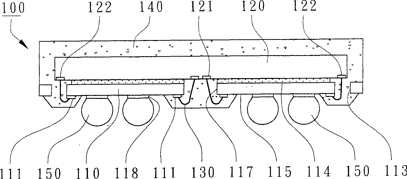
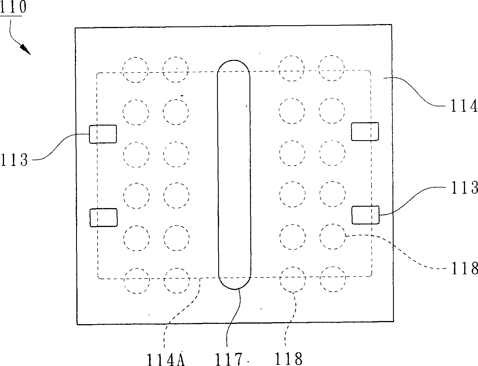
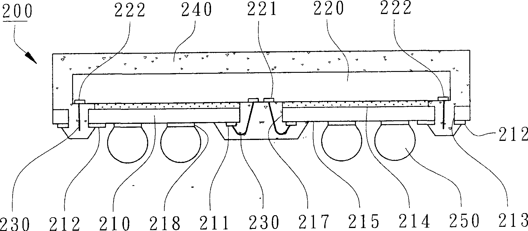
[0069] According to the first preferred embodiment of the present invention, a semico...


PUM


Abstract

The invention relates to a semiconductor packaging structure and base plate used thereby. The semiconductor packaging structure comprises a base plate which has a plurality of signal joint-fingers, a fictitious metal graph and at least a peripheral notch groove penetrating the base plate, a chip which is arranged on the base plate and has a plurality of welding cushions, a plurality of electrically connected elements for connecting the welding cushions of the chip and the signal joint-fingers of the base plate, and a sealed colloid body which is to seal the electrically connected elements and is filled in the peripheral notch groove. The fictitious metal graph extends the trimming to the peripheral notch groove and is electrically insulated from the signal joint-fingers, the base plate has a plurality of signal joint-fingers, the fictitious metal graph and at least a peripheral notch groove penetrating the base plate. Because the peripheral notch groove is favorable for mold flow to fill and reduce the excessive glue of mold seals and the shape of the trimming of the fictitious metal graph to the peripheral notch groove, the invention can inhibit the lateral warping amplitude of the base plate, lower the fracture probability produced by the base plate, and enhance the thermal stress resistance of the peripheral notch groove under the circulation of temperature, thereby avoiding the surface or the lateral sides of the chip from damaging.

Description

technical field [0001] The present invention relates to a window-type semiconductor package structure and its substrate, in particular to a window-opening peripheral, which facilitates mold flow filling and reduces mold overflow, can suppress the warpage of the side of the substrate and reduce the probability of substrate fracture, and can The semiconductor package structure and the substrate used to avoid damage to the surface or side of the chip. Background technique [0002] In the field of integrated circuit packaging, a window type semiconductor package structure (Window type semiconductor package) is to open a through window on the circuit substrate used to carry the chip, so as to allow metal bonding wires or known electrical connection elements to pass through. through the window to electrically connect the substrate and the chip. However, the shape of the conventional window at the center of the substrate should be a long and narrow slot to expose a plurality of ce...

Claims


Application Information

Patent Timeline
Patent Type & Authority Applications(China)
IPC IPC(8): H01L23/488H01L23/498H01L23/13H01L23/31
CPCH01L2224/32225H01L2224/48091H01L2224/4824H01L2224/73215H01L2924/15311
Inventor 范文正刘怡伶
Owner POWERTECH TECHNOLOGY
Why Eureka
Try Eureka