Method of repair of electronic device and repair system

A technology for electronic devices and repair methods, applied in electrical components, printed circuit parts, printed circuit maintenance/correction and other directions, can solve problems such as circuit board distortion, high temperature heating deterioration, and reduce the reliability of solder joints, to suppress distortion, The effect of gentle temperature changes

Inactive Publication Date: 2009-07-15
FUJITSU LTD
View PDF2 Cites 6 Cited by
  • Summary
  • Abstract
  • Description
  • Claims
  • Application Information

AI Technical Summary

Problems solved by technology

The first problem is that the quality of those devices mounted on the surface (second surface) on the opposite side to the surface on which the repair device is mounted will be deteriorated by the high temperature heating of the top heater
[0009] The second problem is that due to the high temperature heating of the bottom heater, the circuit board (made, for example, of fiberglass epoxy) reaches the glass transition temperature (Tg) and the circuit board as a whole will undergo "warping"
This reduces the reliability of solder joints

Method used


Image

  • Method of repair of electronic device and repair system
  • Method of repair of electronic device and repair system
  • Method of repair of electronic device and repair system

Examples


Embodiment Construction

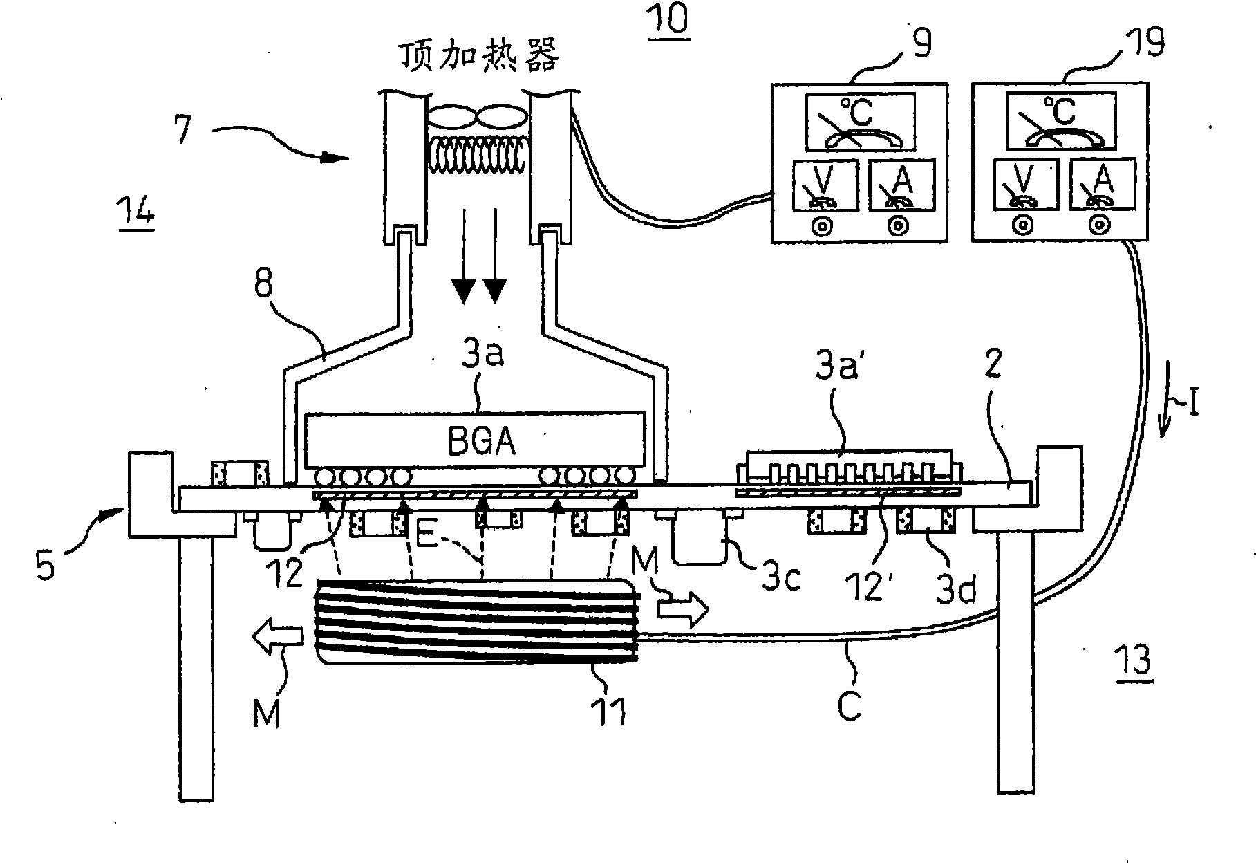
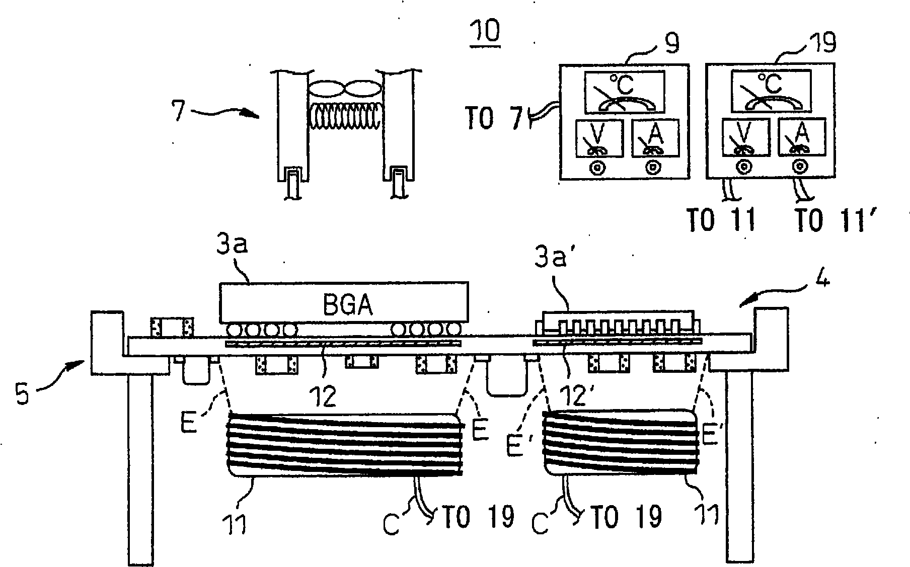
[0037] Before describing the embodiments, the prior art and its disadvantages are described with reference to the related drawings. In order to clarify the effect of the restoration system disclosed here, the conventional restoration system will be described first.

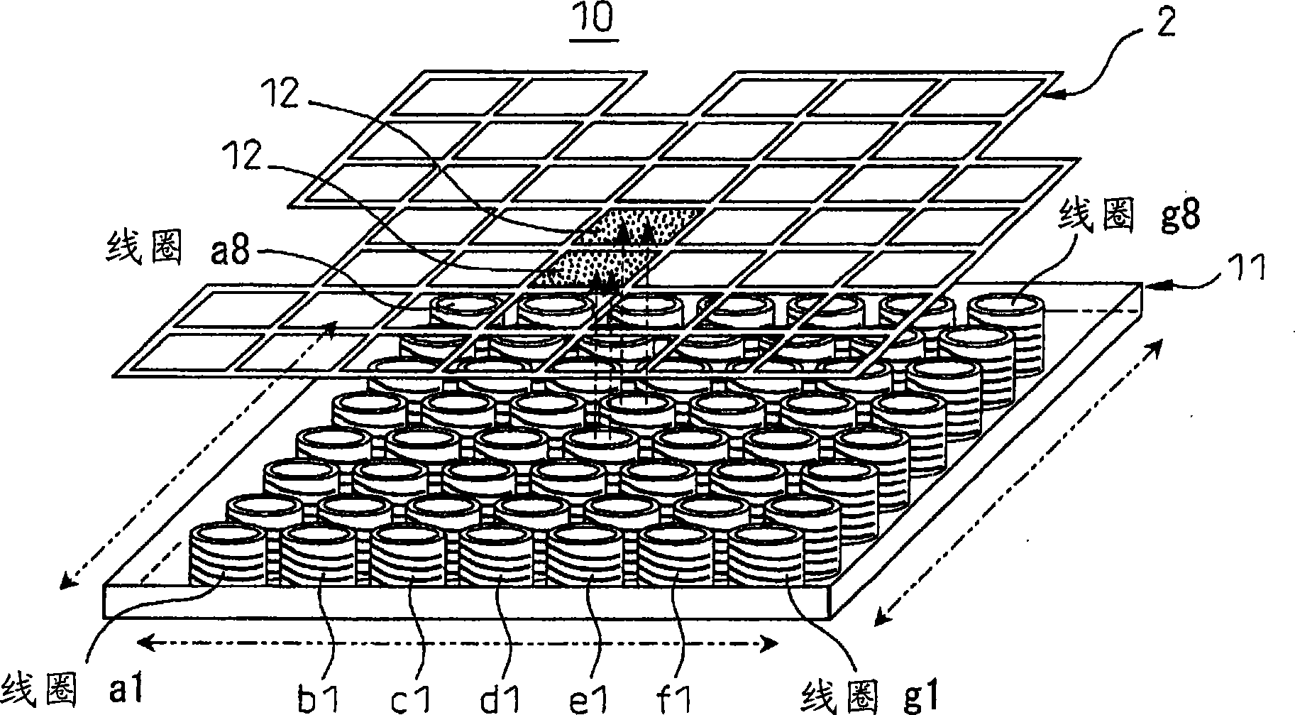
[0038] Figure 15 is a diagram showing a conventional restoration system 1 . In this figure, a plurality of electronic components 3a, 3b are mounted on the first surface (front side) of the circuit board 2 (for simplicity, only three are shown). Among these electronic devices, 3a denotes the above-mentioned BGA as an example of a large-sized device to be repaired (repaired device). 3b, on the other hand, represents an electronic device (IC) that generally does not need to be repaired.

[0039] On the second surface (back) of the circuit board 2 are mounted a plurality of electronic components 3c, 3d (seven are shown for simplicity). Among these electronic devices, 3c denotes an electrolytic capacitor as an exam...


PUM


Abstract

A repair system which prevents heating of weakly heat resistant devices together and causing deterioration of the quality when preheating a first surface of the circuit board, wherein an electromagnetic induction material is buried in advance inside the circuit board near a specific electronic device envisioned as needed repair when becoming a defective electronic device in a production process and an electromagnetic coil emitting electromagnetic waves to an electromagnetic induction member in the vicinity of the repair device is provided and the heat generated by the electromagnetic induction member due to the electromagnetic waves enables the repair device to be heated and detached from the circuit board.

Description

technical field [0001] The present invention relates to a repair method and system for separating an electronic device from a circuit board on which the electronic device is mounted. Background technique [0002] In recent years, the mounting density of electronic components on a circuit board unit including a circuit board on which a plurality of electronic components are mounted has continued to increase. On the other hand, electronic devices are also being developed to accommodate higher densities. One way they have evolved is through the wider use of ball grid arrays (BGAs), chip scale packages (CSPs), and other large-scale electronic devices. These large-sized electronic devices are multi-pin devices. Most of these are structures with multiple sets of terminals on the bottom surface (base surface) of these devices. Since these structures are effective for saving space, they come to be used in large numbers in mobile phones, notebook computers, and the like. [0003]...

Claims


Application Information

Patent Timeline
Patent Type & Authority Applications(China)
IPC IPC(8): H05K3/34H05B6/10B23K3/047B23K1/018
CPCH05K3/225H05K1/0212H05K2203/101H05K3/3494H05K2203/176Y10T29/49137
Inventor 入口慈男畑中清之渡边谕武富信雄山本敬一杉江优
Owner FUJITSU LTD
Why Eureka
Try Eureka