
Method for reducing area of digital logic circuit

A digital logic circuit and area technology, applied in the direction of logic circuits using basic logic circuit components, logic circuits using specific components, etc., can solve problems such as large area

Inactive Publication Date: 2009-07-22
NINGBO UNIV
View PDF0 Cites 11 Cited by
  • Summary
  • Abstract
  • Description
  • Claims
  • Application Information

AI Technical Summary

Problems solved by technology

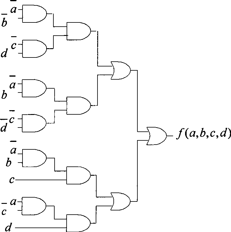
but even for figure 1 The circuit shown is simplified by the method shown in formula (2), and its disadvantage is that the final area is still relatively large and needs to be further reduced

Method used


Image

  • Method for reducing area of digital logic circuit
  • Method for reducing area of digital logic circuit
  • Method for reducing area of digital logic circuit

Examples


Embodiment

[0033] Embodiment: a kind of method for reducing the digital logic circuit area is characterized in that the logic function to be optimized is defined as f; the set of the product term of f is defined as S p ; If S p contains w product terms, any one of which is defined as p i ,D pi represents the product term p i dimension, that is, for a function containing n variables, if a certain product term p of the logic function f i Contains m variables, m≤n, then p i The dimension is D pi =(n-m); the specific steps are:

[0034] a. Define the generalized Hamming distance: For a given function with n variables, remember any two product terms p i ,p j , i≠j, where neither i nor j is greater than w, let x ik represents the product term p i The variable at position k in x jk represents the product term p j The variable at the k-th place in , and let "1" represent the original variable, "0" represent the inverse variable, and "-" represent that the variable does not appear. In ...


PUM


Abstract

The invention discloses a method for reducing the area of a digital logical circuit; a specific product term is generated and added in an optimized function by using characteristics of exclusive OR operation 1 OR 1=0; as the new product term is added, original logically nonadjacent product terms become logically adjacent due to the inserting of added items so as to realize logic optimization; the advantages are as follows: two product terms do not constitute an OR expression right now but an added item p is firstly generated after the two product terms are judged to have a broad hamming distance of 2, and then whether the added item p is fit for simplification of function is judged by a corresponding evaluation method. As the complexity of the logic function is closely related with the complexity of the corresponding digital circuit, simple logic function always corresponds to smaller circuit area, thereby achieving the purpose of reducing the area of digital logic circuit by a method for simplifying the logic function.

Description

technical field [0001] The invention relates to a method for optimizing a digital logic circuit, in particular to a method for reducing the area of ​​a digital logic circuit. Background technique [0002] A very important link in integrated circuit design is the logic synthesis and optimization of the circuit. In logic synthesis and optimization, one of the indicators is how to control the area of ​​the integrated circuit. Considering that the complexity of the logic function is closely related to the complexity of the corresponding digital circuit, a simple logic function often corresponds to a smaller circuit area, so the area of ​​the logic circuit can often be reduced by optimizing the logic function. [0003] The logic function representation of digital circuits can be realized by Boolean logic based on AND / OR / NOT operation, and can also be realized by AND / XOR logic. However, at present, almost all digital Electronic Design Automation (EDA) tools are developed based o...

Claims


Application Information

Patent Timeline
IPC IPC(8): H03K19/173
Inventor 王伦耀夏银水
Owner NINGBO UNIV
Learn More