Drive deivce for TFT LCD
A technology of thin-film transistors and liquid crystal displays, applied in instruments, nonlinear optics, optics, etc., to achieve the effect of reducing smearing
- Summary
- Abstract
- Description
- Claims
- Application Information
AI Technical Summary
Problems solved by technology
Method used
Image
Examples
Embodiment 1
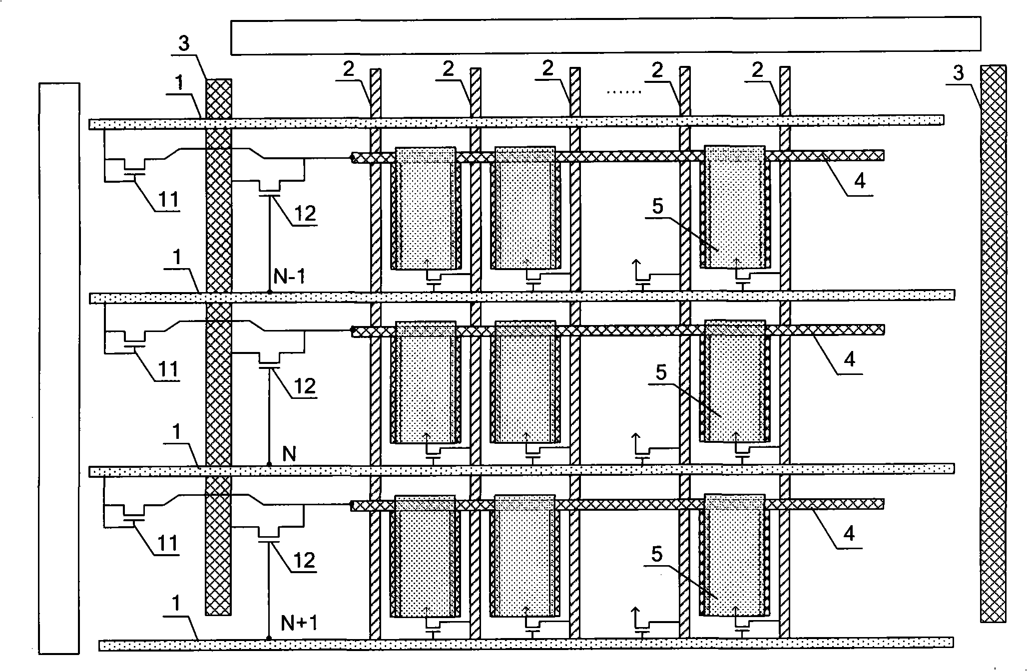
[0029] figure 1 It is the driving equivalent diagram of Embodiment 1 of the driving device of the thin film transistor liquid crystal display of the present invention, as figure 1 As shown, the driving device of the thin film transistor liquid crystal display includes an external common electrode line number line 3 for providing a constant voltage; several pixel common electrode signal lines 4 for maintaining a constant voltage; several gate signal lines 1 for For providing gate signals; several data signal lines 2 are arranged crosswise with several gate signal lines for providing data signals; several pixel electrodes 5, each pixel electrode 5 is located on an adjacent gate signal line Between 1 and the adjacent data signal line 2, it is connected to the drain of the thin film transistor, and the pixel electrode 5 overlaps with the pixel common electrode signal line 4 to form a storage capacitor; several first thin film transistors 11, each first thin film The gate and so...
Embodiment 2
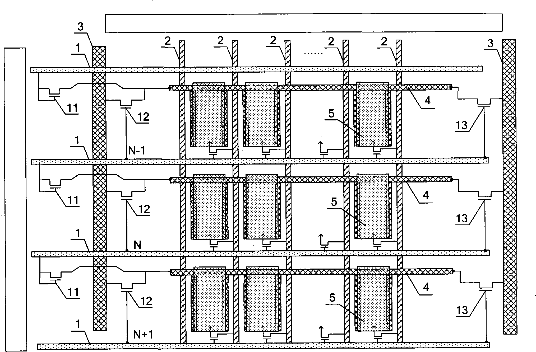
[0033] figure 2 It is the driving equivalent diagram of Embodiment 2 of the driving device of the thin film transistor liquid crystal display of the present invention, as figure 2 As shown, different from Embodiment 1, further, the driving device of the thin film transistor liquid crystal display of the present invention further includes: several third thin film transistors 13, the gate of each third thin film transistor 13 and the gate signal line 1 The two terminals are connected, the source is connected to the external common electrode signal line 3 , and the drain is connected to the second end of the pixel common electrode signal line 4 .
[0034] Take the n-1, n, and n+1 lines as an example for illustration. When the n-th line is turned on, that is, when the gate signal line 1 applies a high-voltage signal (Vgh), the pixel electrode 5 of the n-th line is introduced into the data signal line 2 for transmission. Since the other rows are under the control of the low volt...
Embodiment 3
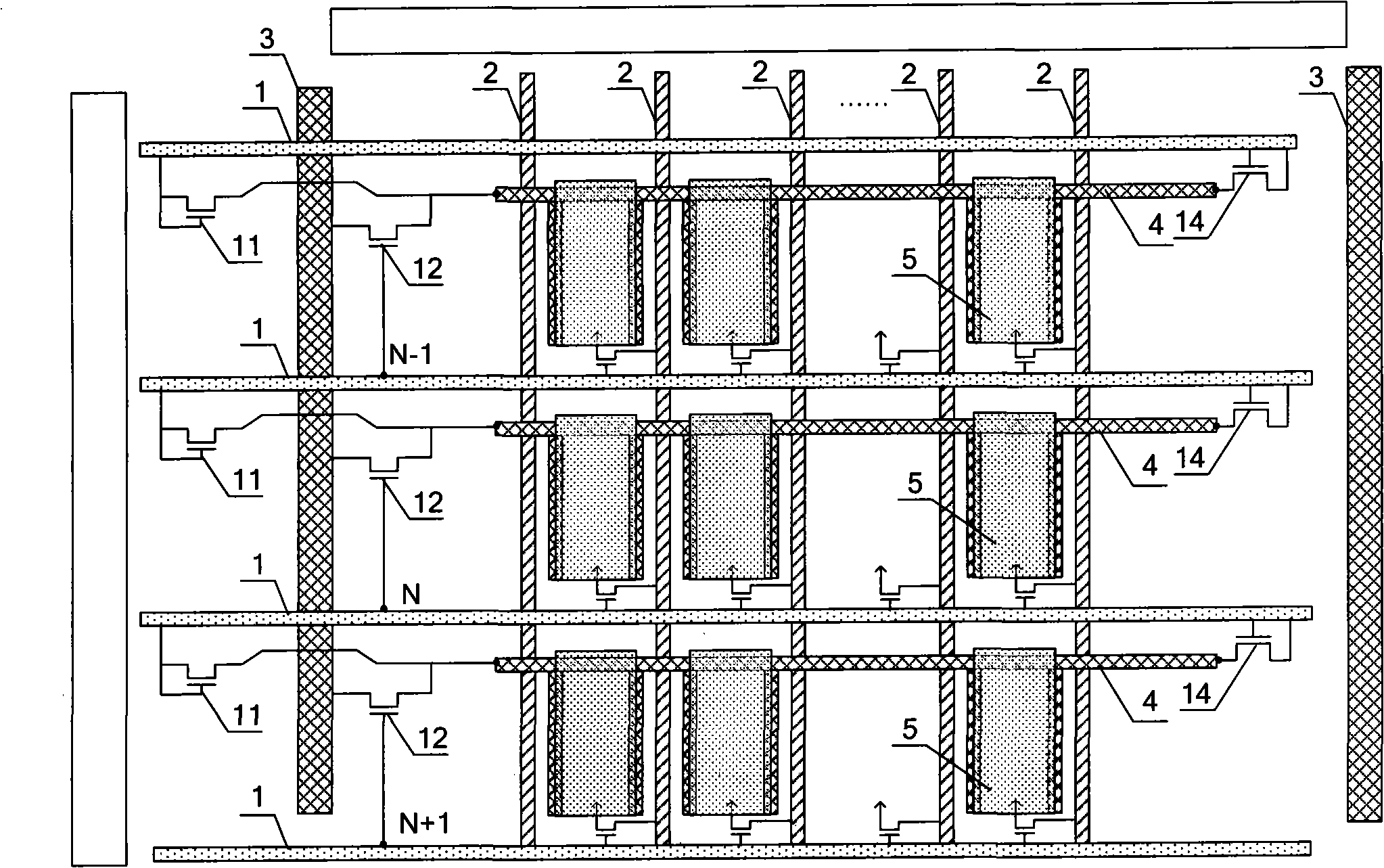
[0037] image 3 It is the driving equivalent diagram of Embodiment 3 of the driving device of the thin film transistor liquid crystal display of the present invention, such as image 3 As shown, different from Embodiment 1, further, the driving device of the thin film transistor liquid crystal display of the present invention also includes: several fourth thin film transistors 14, and the gate and source of each fourth thin film transistor 14 are connected with those of the previous row. The gate signal line 1 is connected to the second end, and the drain is connected to the second end of the pixel common electrode signal line 4 .
[0038] Take the n-1, n, and n+1 lines as an example for illustration. When the n-th line is turned on, that is, when the gate signal line 1 applies a high-voltage signal (Vgh), the pixel electrode 5 of the n-th line is introduced into the data signal line 2 for transmission. Since the other rows are controlled by the low voltage signal (Vgl), the ...
PUM
 Abstract
Description
Claims
Application Information
 - R&D
- Intellectual Property
- Life Sciences
- Materials
- Tech Scout
- Unparalleled Data Quality
- Higher Quality Content
- 60% Fewer Hallucinations
Browse by: Latest US Patents, China's latest patents, Technical Efficacy Thesaurus, Application Domain, Technology Topic, Popular Technical Reports.
© 2025 PatSnap. All rights reserved.Legal|Privacy policy|Modern Slavery Act Transparency Statement|Sitemap|About US| Contact US: help@patsnap.com


