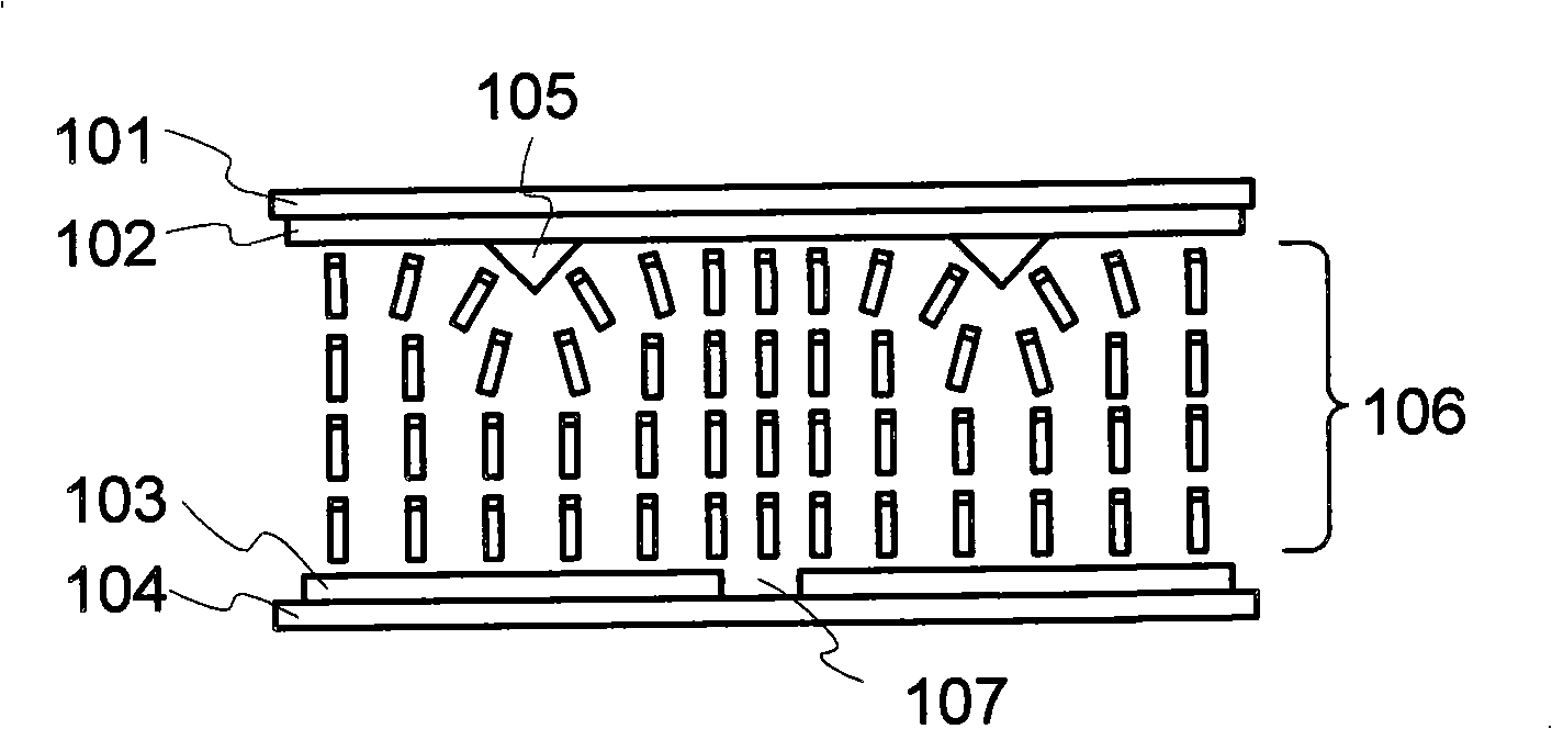
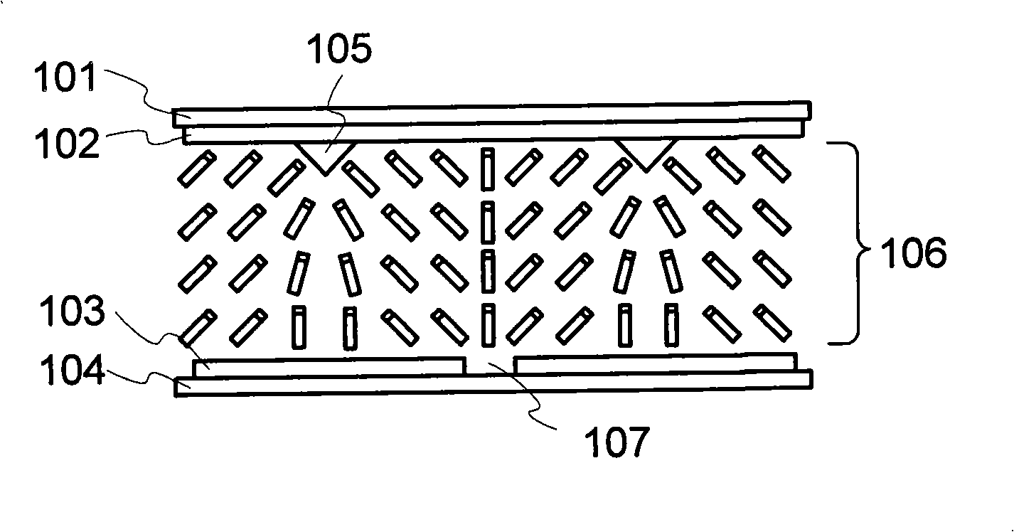
Pixel circuit of LCD device in vertical orientation mode
A technology of a liquid crystal display device and a vertical alignment mode, which is applied in the field of pixel circuits, and can solve problems such as inflexible adjustment of gamma characteristics, decreased pixel aperture ratio, complex pixels, etc., to improve display quality, increase contrast, and adjust gamma characteristics Effect
- Summary
- Abstract
- Description
- Claims
- Application Information
AI Technical Summary
Problems solved by technology
Method used
Image

Examples
Embodiment 1
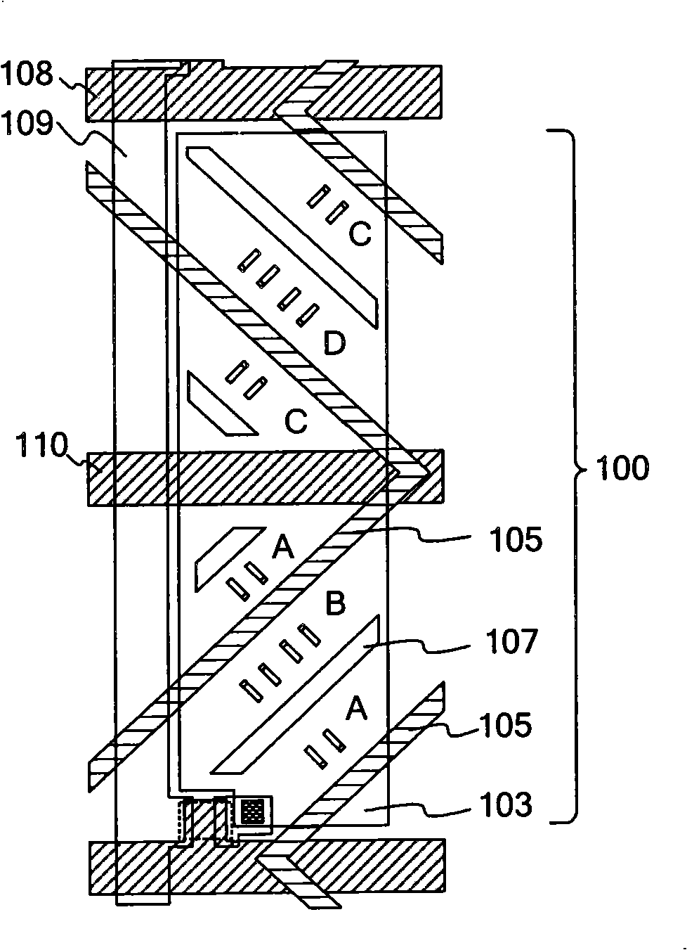
[0055] refer to Figure 5 (a), the pixel circuit of the vertical alignment mode liquid crystal display device includes the first gate line GL1 and the second gate line GL2 extending in the first direction, the first data line DL1 and the second data line DL2 extending in the second direction , the first thin film transistor T1, the second thin film transistor T2, the storage capacitor C ST , LCD capacitance C LC ; The first thin film transistor T1 and the second thin film transistor T2 are respectively controlled by the first gate line GL1 and the second gate line GL2 which transmit the scanning signal, and the storage capacitor C ST , LCD capacitance C LC The first thin film transistor T1 and the second thin film transistor T2 are respectively connected to the first data line DL1 and the second data line DL2; that is, the gate electrodes of the first thin film transistor T1 and the second thin film transistor T2 are respectively connected to the first gate line GL1 and the...
Embodiment 2
[0058] refer to Figure 6 (a), the pixel circuit of the vertical alignment mode liquid crystal display device is also provided with an additional capacitor for charge sharing, and the thin film transistors include a first thin film transistor T1, a second thin film transistor T2, and a third thin film transistor T3, and the first thin film transistor T3 1. The gate electrodes of the third thin film transistors T1 and T3 are electrically connected to the first gate line GL1, the source electrode of the first thin film transistor T1 is electrically connected to the data line DL, and the gate electrode of the second thin film transistor T2 is electrically connected to the second gate line. The line GL2 is electrically connected, that is, the first thin film transistor T1 and the third thin film transistor T3 are controlled by the first gate line GL1 that transmits the scanning signal, and the second thin film transistor T2 is controlled by the second gate line GL2 that transmits t...
Embodiment 3
[0063] refer to Figure 7 (a), the pixel circuit of the vertical alignment mode liquid crystal display device is provided with a thin film transistor T, which is controlled by the gate line GL which transmits the scanning signal. There is a storage capacitor C in the pixel circuit ST , LCD capacitance C LC . Among them, the liquid crystal capacitance C LC It is connected to the data line DL through a thin film transistor T.
[0064] refer to Figure 7 (b), the horizontal axis t of the coordinates represents time, and the vertical axis V GL Indicates the voltage signal on the gate line GL, V DL Indicates the voltage signal on the data line DL. In one modulation cycle, that is, within one frame time, there are two data signal writing processes, that is, the gate line GL controls the thin film transistor T to turn on at different time points within one frame time, and input voltage signals respectively, so that the liquid crystal capacitance C LC Different signal voltage...
PUM
 Abstract
Description
Claims
Application Information
 - R&D
- Intellectual Property
- Life Sciences
- Materials
- Tech Scout
- Unparalleled Data Quality
- Higher Quality Content
- 60% Fewer Hallucinations
Browse by: Latest US Patents, China's latest patents, Technical Efficacy Thesaurus, Application Domain, Technology Topic, Popular Technical Reports.
© 2025 PatSnap. All rights reserved.Legal|Privacy policy|Modern Slavery Act Transparency Statement|Sitemap|About US| Contact US: help@patsnap.com