
Charge pumping circuit

A charge pumping and pumping technology, applied in the direction of adjusting electrical variables, control/regulation systems, instruments, etc., can solve the problems of increasing cost, reducing the maximum load capacity, increasing circuit cost, etc., achieving high efficiency, saving quantity, and load The effect of high current

Inactive Publication Date: 2010-11-03
NOVATEK MICROELECTRONICS CORP
View PDF4 Cites 1 Cited by
  • Summary
  • Abstract
  • Description
  • Claims
  • Application Information

AI Technical Summary

Problems solved by technology

[0007] For the charge pump circuit, the built-in (build-in) capacitor will occupy a large area of ​​the integrated circuit (Integral circuit, IC), increasing the cost
The external capacitor components will increase the area of ​​the circuit board, which will also increase the cost and hinder the miniaturization of the product.
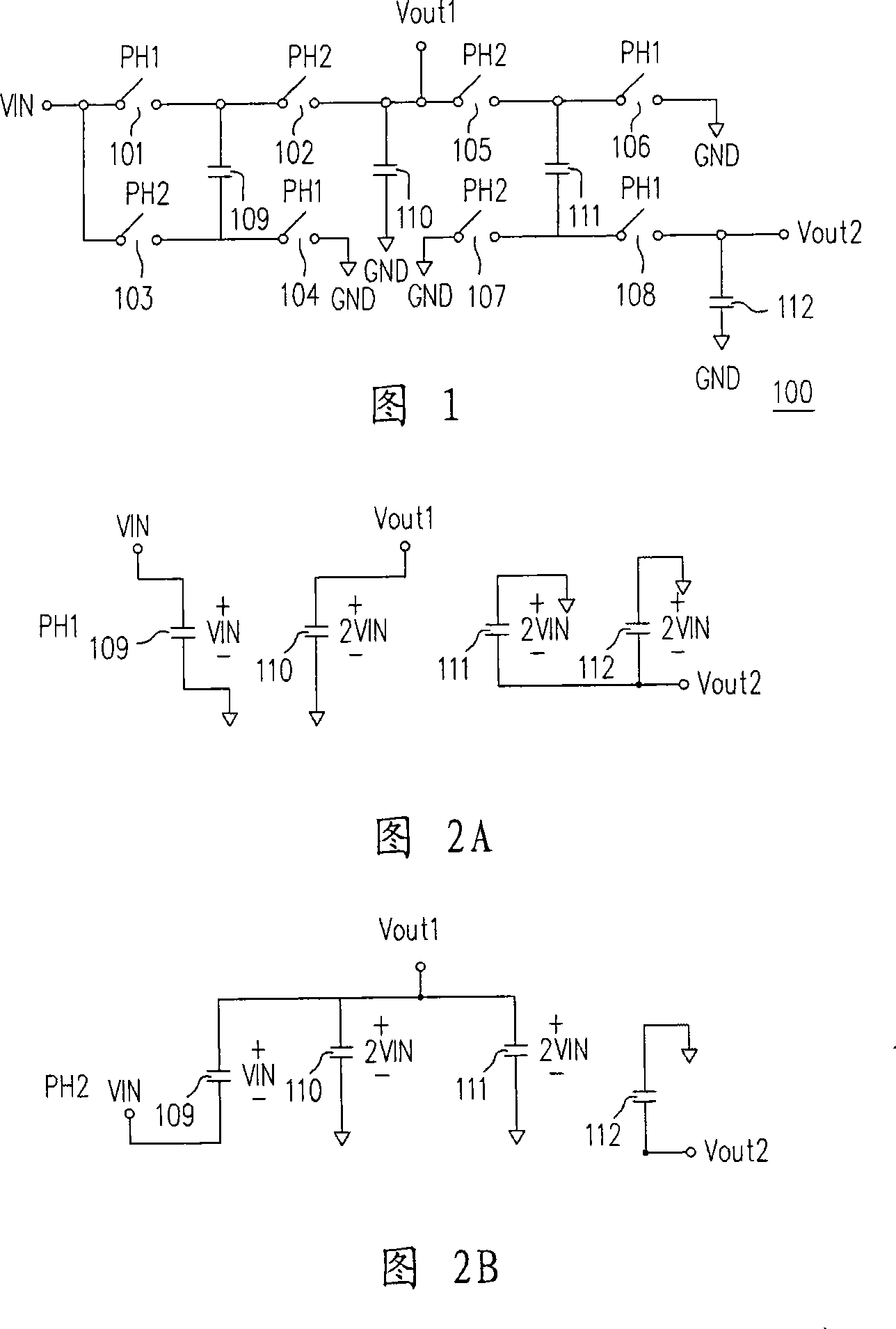
Although the known charge pump circuit 100 can generate output voltages of 2VIN and -2VIN, the output voltages Vout1 and Vout2 both require a voltage stabilizing capacitor, thus increasing the cost of the circuit
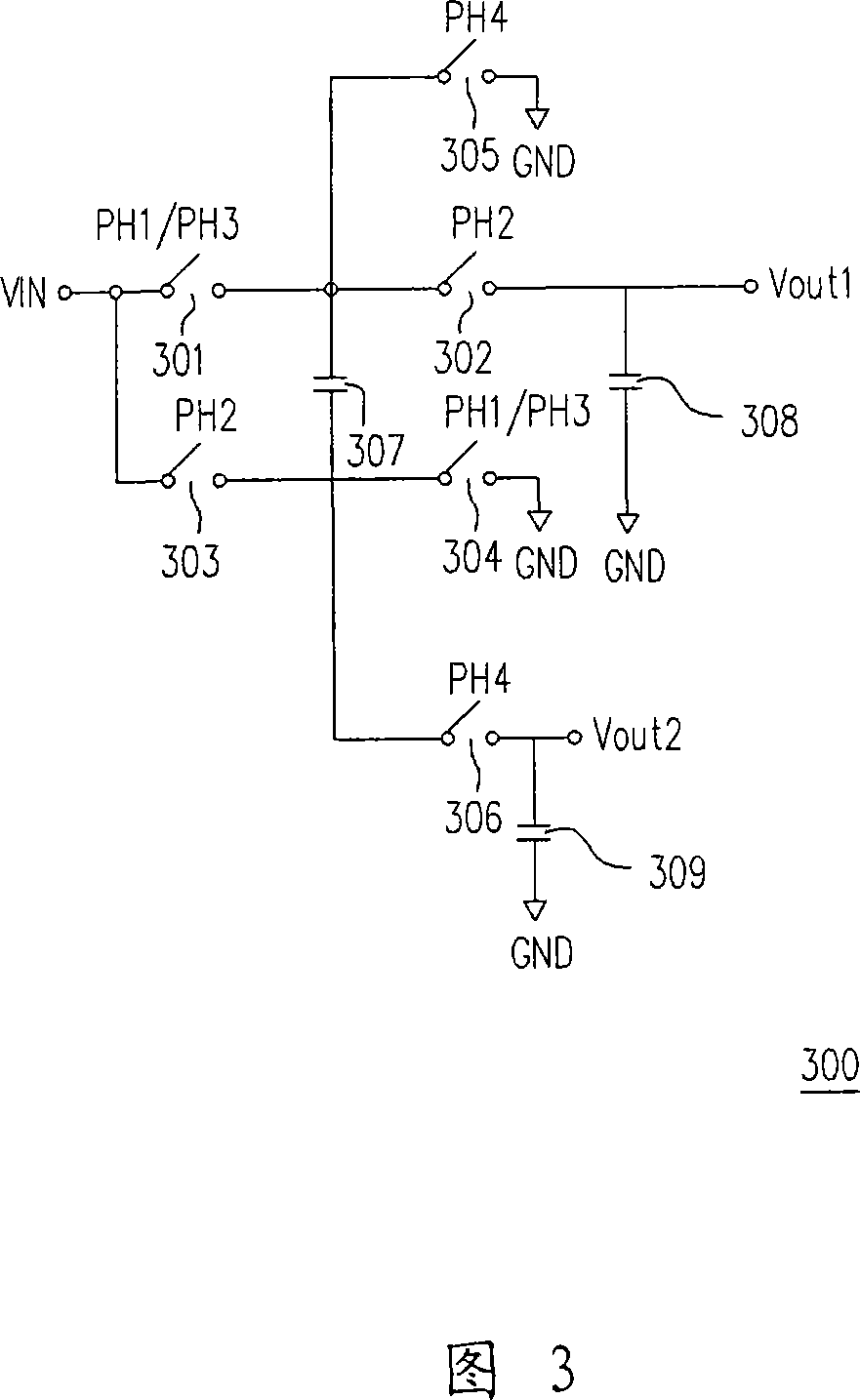
In addition, although the known charge pump circuit 300 has one capacitor less than the charge pump circuit 100, the most negative voltage generated is only -VIN
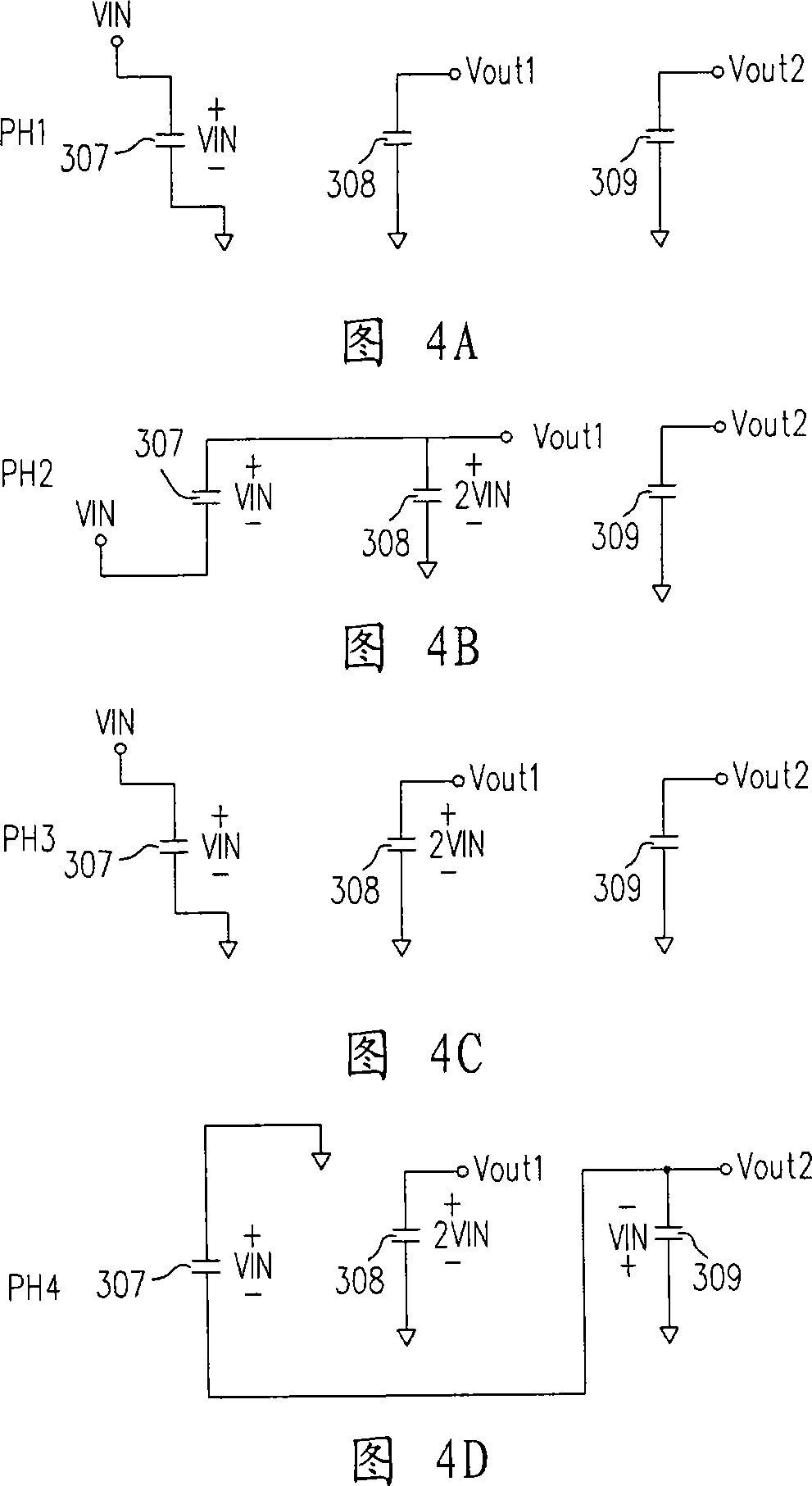
However, the charge pump circuit 300 uses 4 control signals (4 periods) to generate output voltages of 2VIN and -VIN, which will reduce the efficiency of the charge pump circuit 300 and reduce the maximum load capacity.

Method used


Image

  • Charge pumping circuit
  • Charge pumping circuit
  • Charge pumping circuit

Examples


no. 1 example

[0053] Figure 5 A circuit diagram of the charge pump of the first embodiment of the present invention is shown. The charge pumping circuit 500 includes a pumping unit 510, a first switch SW1, a second switch SW2, a third switch SW3, a fourth switch SW4, a fifth switch SW5, a sixth switch SW6, a storage capacitor (fly capacitor) Cf2 and Output capacitor Cout.

[0054] The first terminal T1 of the pumping unit 510 is coupled to the input voltage Vin, and the second terminal T2 thereof is coupled to the first voltage V1 (for example, the ground voltage GND). The pumping unit 510 also includes an internal capacitor Cf1, a seventh switch SW7 and an eighth switch SW8. The first terminal of the seventh switch SW7 is the first terminal T1 of the pumping unit 510, and the second terminal thereof is coupled to the first terminal of the internal capacitor Cf1, wherein the first terminal of the internal capacitor Cf1 is the first terminal of the pumping unit 510. Four-terminal T4. Th...

no. 2 example

[0062] Figure 7 A circuit diagram of a charge pump according to a second embodiment of the present invention is shown. Please refer to Figure 7 , the charge pumping circuit 700 includes a pumping unit 710, a first switch SW1, a second switch SW2, a third switch SW3, a fourth switch SW4, a fifth switch SW5, a sixth switch SW6, a storage capacitor (fly capacitor) Cf2 with output capacitor Cout.

[0063] A first terminal of the first switch SW1 is coupled to the second voltage V2 (for example, the input voltage Vin), and a second terminal thereof is coupled to the third terminal T3 of the pumping unit 710 . The first terminal of the second switch SW2 is coupled to the fourth terminal T4 of the pumping unit 710 . A first terminal of the third switch SW3 is coupled to a second terminal of the second switch SW2. Wherein, the first terminal of the third switch SW3 is coupled to the output terminal of the first output voltage VO1 . The first terminal of the fourth switch SW4 is...

no. 3 example

[0072] Figure 8 A circuit block diagram of a charge pump according to a third embodiment of the present invention is shown. Please refer to Figure 8 , the charge pumping circuit 800 includes a pumping unit 810, a first switch SW1, a second switch SW2, a third switch SW3, a fourth switch SW4, a fifth switch SW5, a storage capacitor Cf2 and an output capacitor Cout. The pump unit 810 has an input terminal and an output terminal TO1. Wherein, the input terminal of the pumping unit 810 receives the input voltage Vin, and provides the first output voltage VO1 at the output terminal TO1 of the pumping unit 810 .

[0073] A first terminal of the first switch SW1 is coupled to the output terminal TO1 of the pumping unit 810 . Wherein, the second terminal of the first switch SW1 is coupled to the output terminal of the first output voltage VO1 . A first terminal of the second switch SW2 is coupled to a second terminal of the first switch SW1 . The first terminal of the third swi...


PUM


Abstract

A charge pumping circuit comprises a pumping unit, first to sixth switches, a fly capacitor and an output capacitor, wherein, for a first phase, an input voltage and a first voltage respectively get access to a first end and a second end of the pumping unit to charge at least one capacitor inside the pumping unit; for a second phase, the internal capacitor of the pumping unit provides charge to the fly capacitor to generate a first output voltage through the second switch on the basis of a second voltage level through the first switch; and for a third phase, the fly capacitor provides charge to the output capacitor to generate a second output voltage through the sixth switch on the basis of a third voltage level through the third switch.

Description

technical field [0001] The invention relates to a charge pumping circuit, in particular to a charge pumping circuit with reduced capacitance components. Background technique [0002] In electronic circuits, voltages of various levels are often required for circuit use. Therefore, electronic circuits are often configured with charge pump circuits to generate voltages of various levels. [0003] figure 1 A circuit diagram of a known charge pump is shown. Please refer to figure 1 , the charge pumping circuit 100 includes switches 101 - 108 and capacitors 109 - 112 . The charge pump circuit 100 uses two control signals PH1 (first period) and PH2 (second period) to control the on and off states of the switches 101 - 108 in turn. When the control signal PH1 is at a high level, the switches 101, 104, 106 and 108 are turned on, and the equivalent circuit of the charge pumping circuit 100 is shown as Figure 2A shown. At this time, the input voltage VIN charges the capacitor 1...

Claims


Application Information

Patent Timeline
Patent Type & Authority Patents(China)
IPC IPC(8): G05F3/02
Inventor 谢致远颜志仁
Owner NOVATEK MICROELECTRONICS CORP
Learn More