Substrate for mounting device, semiconductor module and method for producing the same, and portable apparatus
A technology for installation and components, which is applied in semiconductor/solid-state device manufacturing, semiconductor devices, semiconductor/solid-state device components, etc., which can solve the problems of insulating resin peeling, increased number of manufacturing processes, and low adhesion between insulating resin and semiconductor components
- Summary
- Abstract
- Description
- Claims
- Application Information
AI Technical Summary
Problems solved by technology
Method used
Image

Examples
Embodiment approach 1
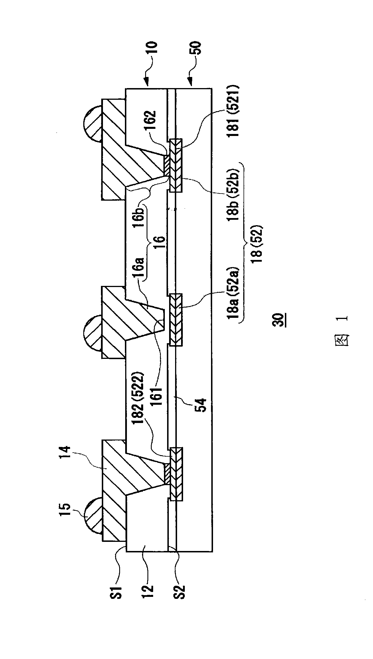
[0045] 1 is a schematic cross-sectional view showing the structure of a component mounting substrate 10 and a semiconductor package 30 using the same according to Embodiment 1. As shown in FIG. The semiconductor package 30 has a substrate 10 for mounting an element and a semiconductor element 50 mounted on the substrate 10 for mounting an element.
[0046] The component mounting substrate 10 has: an insulating resin layer 12 formed of an insulating resin; a wiring layer 14 provided on one main surface S1 of the insulating resin layer 12; electrically connected to the wiring layer 14 and insulated from the wiring layer 14; A plurality of protruding electrodes 16 protruding from the side of the resin layer 12 . In addition, the component mounting substrate 10 has a counter electrode 18 provided on the other main surface S2 of the insulating resin layer 12 at positions corresponding to the plurality of protruding electrodes 16, and has a top portion corresponding to the protrudin...
Embodiment approach 2
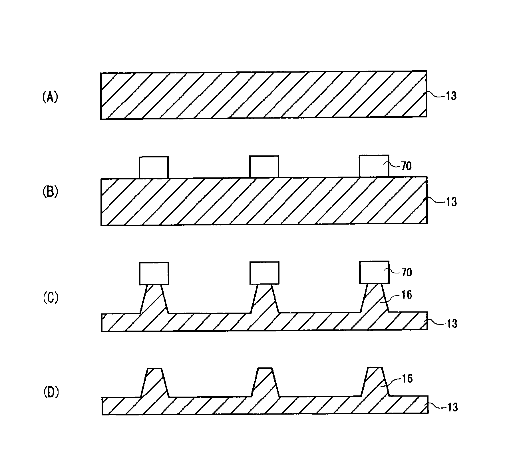
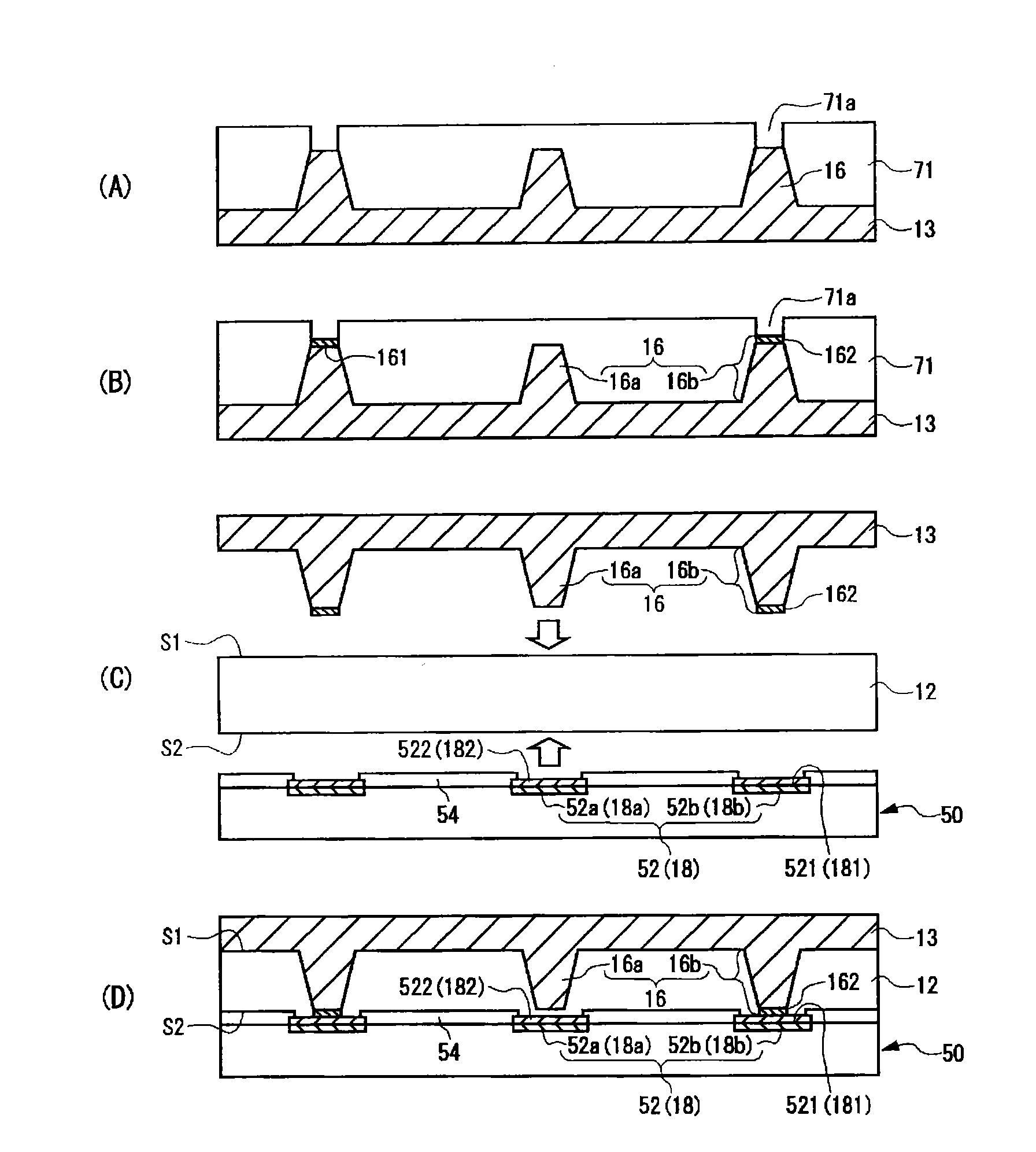
[0073] In Embodiment 1 above, the insulating resin layer 12 is sandwiched between the copper plate 13 and the counter electrode 18 or the semiconductor element 50, and the insulating resin layer 12 is press-molded to integrate them to form the element mounting substrate 10 or the semiconductor package 30. However, The element mounting substrate 10 or the semiconductor package 30 may also be formed as follows. This embodiment will be described below. The method of forming the protruding electrodes 16 is the same as that of the first embodiment. In addition, the same reference numerals are assigned to the same configurations as those in Embodiment 1, and description thereof will be omitted.
[0074] Figure 5 (A)~(F) and Figure 6 (A) to (C) are process cross-sectional views showing a method of bonding the protruding electrode 16 to the counter electrode 18 or the element electrode 52 .
[0075] Such as Figure 5 As shown in (A), on the main surface of the copper plate 13 o...
Embodiment approach 3
[0086] In the configurations of Embodiments 1 and 2, the insulating resin layer 12 is present between the protruding electrode 16a and the opposing electrode 18a or the element electrode 52a. A dielectric film layer having a dielectric constant larger than that of the insulating resin layer 12 is provided between the electrodes 18a or the element electrodes 52a. This embodiment will be described below. Incidentally, the method of forming the protruding electrodes 16 is the same as that of the first embodiment. In addition, the same code|symbol is attached|subjected to the same structure as Embodiment 1 or 2, and description is abbreviate|omitted.
[0087] Figure 7 (A)~(G) and Figure 8 (A) to (E) are process cross-sectional views showing a method of bonding the protruding electrode 16 to the counter electrode 18 or the element electrode 52 .
[0088] Such as Figure 7 As shown in (A), the dielectric film 20 is formed on the entire main surface of the copper plate 13 on t...
PUM
| Property | Measurement | Unit |
|---|---|---|
| Thickness | aaaaa | aaaaa |
| Thickness | aaaaa | aaaaa |
| Thickness | aaaaa | aaaaa |
Abstract
Description
Claims
Application Information
 - R&D
- Intellectual Property
- Life Sciences
- Materials
- Tech Scout
- Unparalleled Data Quality
- Higher Quality Content
- 60% Fewer Hallucinations
Browse by: Latest US Patents, China's latest patents, Technical Efficacy Thesaurus, Application Domain, Technology Topic, Popular Technical Reports.
© 2025 PatSnap. All rights reserved.Legal|Privacy policy|Modern Slavery Act Transparency Statement|Sitemap|About US| Contact US: help@patsnap.com