

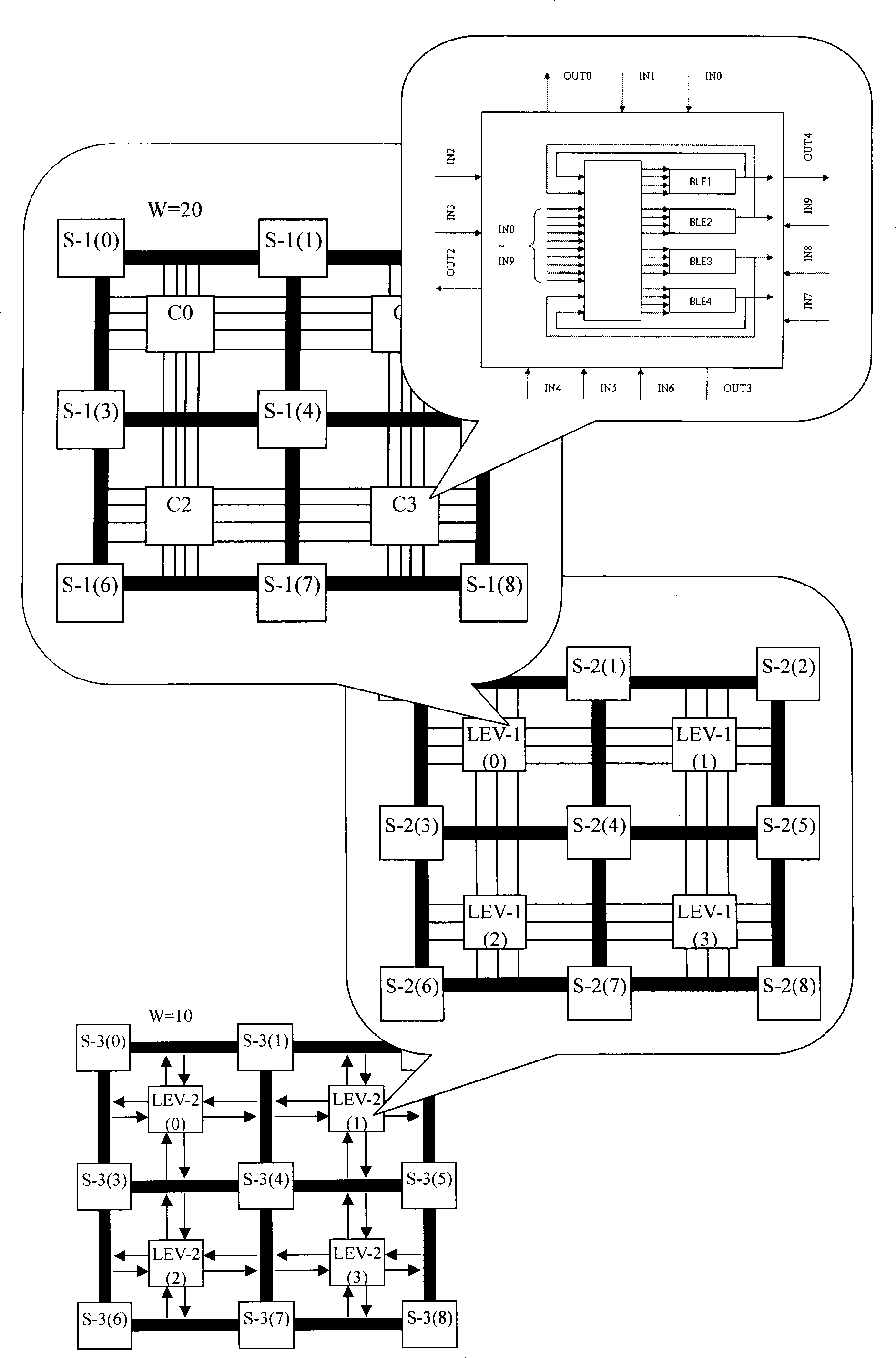
Multi-hierarchy FPGA
A multi-level, low-level technology, applied in the direction of logic circuits using basic logic circuit components, logic circuits using specific components, etc., can solve the problems of insufficient use of chip wiring resources and large wiring delays, and achieve high integration and reliability. The effect of miniaturization, good delay characteristics, and improved utilization efficiency
- Summary
- Abstract
- Description
- Claims
- Application Information
AI Technical Summary
Problems solved by technology
Method used
Image

Examples
Embodiment
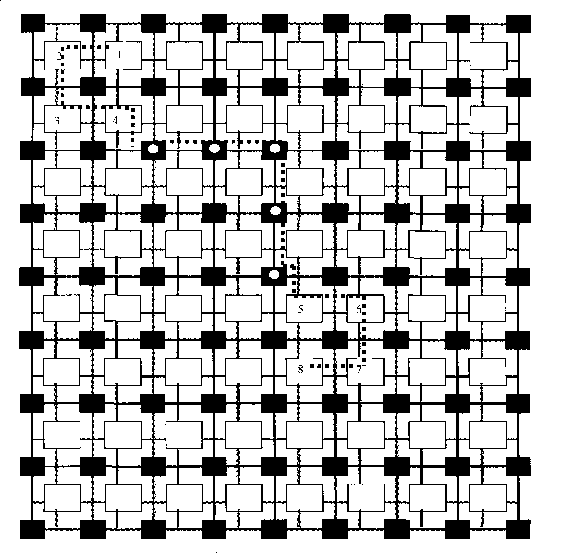
[0021] In order to compare the pros and cons of island FPGAs and Multi-level FPGAs in terms of latency and area, consider the following examples.
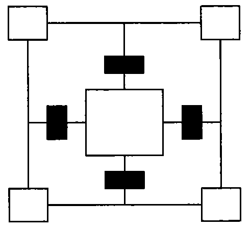
[0022] An 8-bit full adder is implemented with the isolated island FPGA and the multi-level FPGA of the present invention respectively. In the 8-bit full adder, let the input two sets of 8-bit data be A1, A2, A3, A4, A5, A6, A7 and B1, B2, B3, B4, B5, B6, B7, and the carry is Cin. Each CLB can implement a one-bit adder, so 8 CLBs are required. Figure 1 shows the 8 CLBs used by the isolated island FPGA. Such a distribution is more likely to be distributed in practical applications. Figure 1a , black squares represent SBs, white squares represent CLBs, and lines between black squares represent channels. CLBs and channels are connected by CBs. There are two CBs between every two CLBs. CBs are in Figure 1a not shown in the Figure 1b is represented as a black rectangle. Each CLB can be regarded as a 1-bit full adder, using 3 inputs ...
PUM
 Abstract
Description
Claims
Application Information