
Bond pad structure

A technology of welding pads and conductive structures, which is applied in the direction of semiconductor/solid-state device parts, semiconductor devices, electrical components, etc., and can solve problems such as damage

Active Publication Date: 2011-01-26
TAIWAN SEMICON MFG CO LTD
View PDF0 Cites 0 Cited by
  • Summary
  • Abstract
  • Description
  • Claims
  • Application Information

AI Technical Summary

Problems solved by technology

Stress from soldering, electrical testing, and other possible stressors can cause damage to the pad structure as well as the underlying

Method used


Image

  • Bond pad structure
  • Bond pad structure
  • Bond pad structure

Examples


Embodiment Construction

[0018] It should be understood that the following description provides many different embodiments or examples in order to achieve different features of the invention. The components and structures of certain examples are described below for the purpose of simplifying the present disclosure. Of course, they are only examples and should not be limiting. Furthermore, in different embodiments, the present disclosure may repeat reference numerals and / or letters. These repetitions are for the purpose of simplification and clarification, and are not inherently intended to indicate a relationship between the different embodiments and / settings discussed. In addition, in the following description, the formation of the first feature on or over the second feature may include an embodiment in which the first feature and the second feature are in direct contact, and may also include an embodiment that is formed between the first feature and the second feature. An embodiment of an addition...


PUM


Abstract

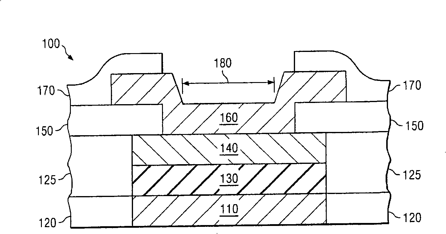
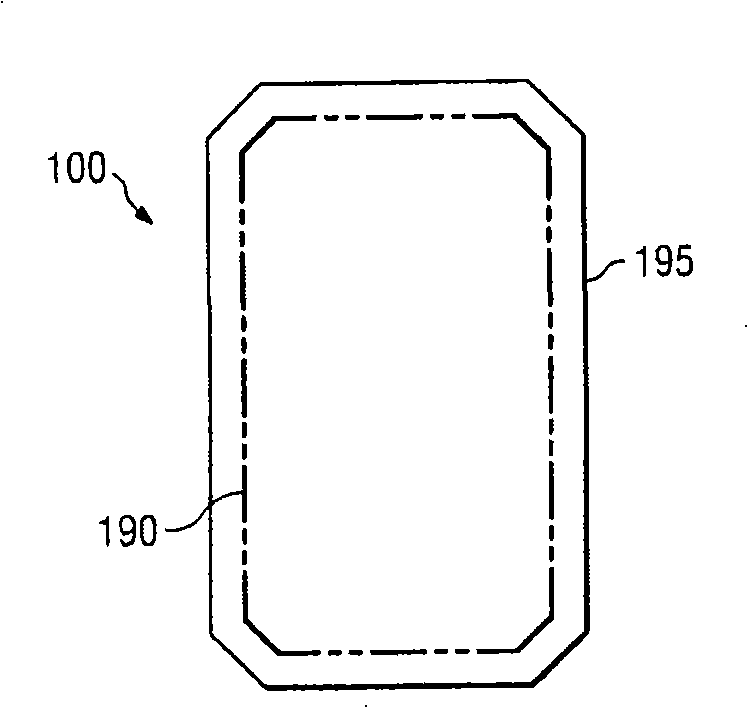
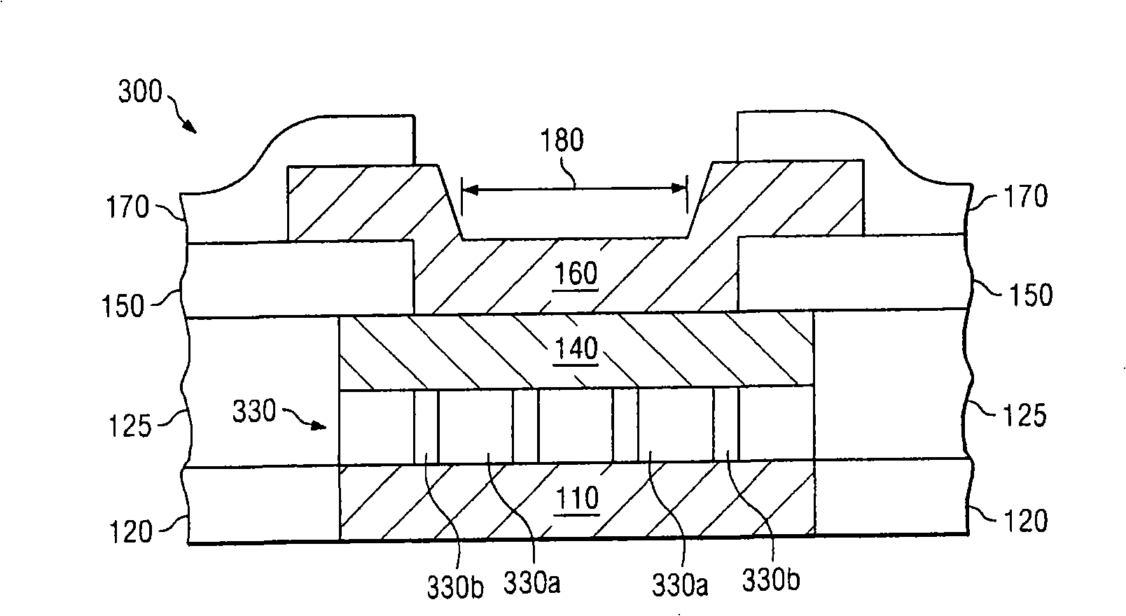
A bonding pad structure is provided that includes two conductive layers and a connective layer interposing the two conductive layers. The connective layer includes a contiguous, conductive structure. In an embodiment, the contiguous conductive structure is a solid layer of conductive material. In other embodiments, the contiguous conductive structure is a conductive network including, for example, a matrix configuration or a plurality of conductive stripes. At least one dielectric spacer may interpose the conductive network. In an embodiment, the conductive density of the connective layer is between approximately 20% and 100%.

Description

technical field [0001] The present invention generally relates to integrated circuits, and more particularly to a pad structure. Background technique [0002] Integrated circuits are typically formed on substrates such as semiconductor wafers. Bonding pads are included on the substrate, the pads providing contact surfaces to the integrated circuit device whereby electrical connections can be made to the integrated circuit device. Conventional techniques such as thermocompression or thermosonic wire bonding, flip chip techniques, and other techniques known in the art may be used to provide connections from the package terminals to the integrated circuit using pads. [0003] Interconnection technology can cause mechanical stress on the pad structure and the surrounding area, for example from the position of the ball or wedge joint in the wire bonding process or from the bump to the solder joint in the flip chip technology. Pad. Additionally, the pads may be used to provide ...

Claims


Application Information

Patent Timeline
Patent Type & Authority Patents(China)
IPC IPC(8): H01L23/485
CPCH01L2224/85205H01L2924/01014H01L2924/04953H01L2924/01074H01L2224/05184H01L2924/01027H01L2924/30105H01L2924/01087H01L2224/05624H01L2224/05187H01L2924/01029H01L2224/16H01L24/05H01L2224/05166H01L2224/05093H01L2224/05147H01L2924/01013H01L2924/05042H01L2924/01082H01L2924/01033H01L2924/01028H01L2924/01046H01L2924/01049H01L2224/05124H01L2924/10329H01L2924/3011H01L2924/04941H01L2224/05558H01L2224/05181H01L2224/05096H01L2924/10253H01L2224/05552H01L2224/85201H01L2924/01006H01L2924/01022H01L2924/01032H01L2924/01078H01L2924/01073H01L2924/01019H01L2224/05556H01L2924/14H01L2924/01068H01L2224/02166H01L2224/0401H01L2924/00012H01L2924/00H01L24/03H01L2924/37001
Inventor 郑心圃刘豫文蔡豪益陈宪伟
Owner TAIWAN SEMICON MFG CO LTD
Learn More