Surface coarsening LED chip and manufacturing method thereof

A technology for light-emitting diodes and surface roughening, which is applied in the fields of light-emitting diode chips, chip manufacturing, and light-emitting diode chip manufacturing. It can solve the problem of heat dissipation of high-power light-emitting diodes and improve light efficiency. Low efficiency and other problems, to avoid visible light resonance, improve external quantum efficiency, and reduce the number of total reflections

Inactive Publication Date: 2009-08-26
HE SHAN LIDE ELECTRONICS ENTERPRISE CO LTD
View PDF0 Cites 13 Cited by
  • Summary
  • Abstract
  • Description
  • Claims
  • Application Information

AI Technical Summary

Problems solved by technology

Therefore, the manufacture of this chip has the defects of short life and low light extraction efficiency.
[0005] With the continuous improvement of chip manufacturing capabilities, the luminous efficiency and brightness required by light-emitting diodes continue to increase. Traditional chip manufacturing processes can no longer solve the heat dissipation problem of high-power light-emitting diodes and the technical problems of improving light efficiency. High-power light-emitting diodes are also gradually Instead of traditional low-power light-emitting diodes, the structure of high-power chip epitaxy is the same as that of traditional light-emitting diodes, but the chip manufacturing process is not the same

Method used


Image

  • Surface coarsening LED chip and manufacturing method thereof
  • Surface coarsening LED chip and manufacturing method thereof
  • Surface coarsening LED chip and manufacturing method thereof

Examples


Embodiment Construction

[0037] Embodiments of the present invention will now be described in detail by way of examples with reference to the accompanying drawings.

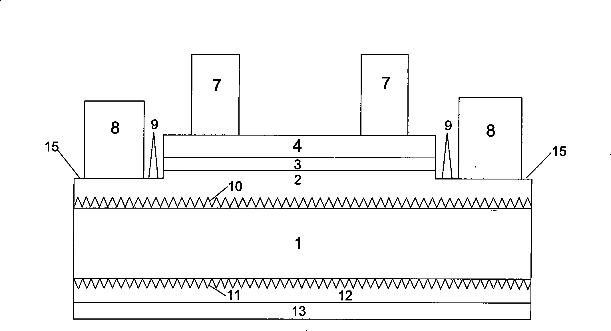
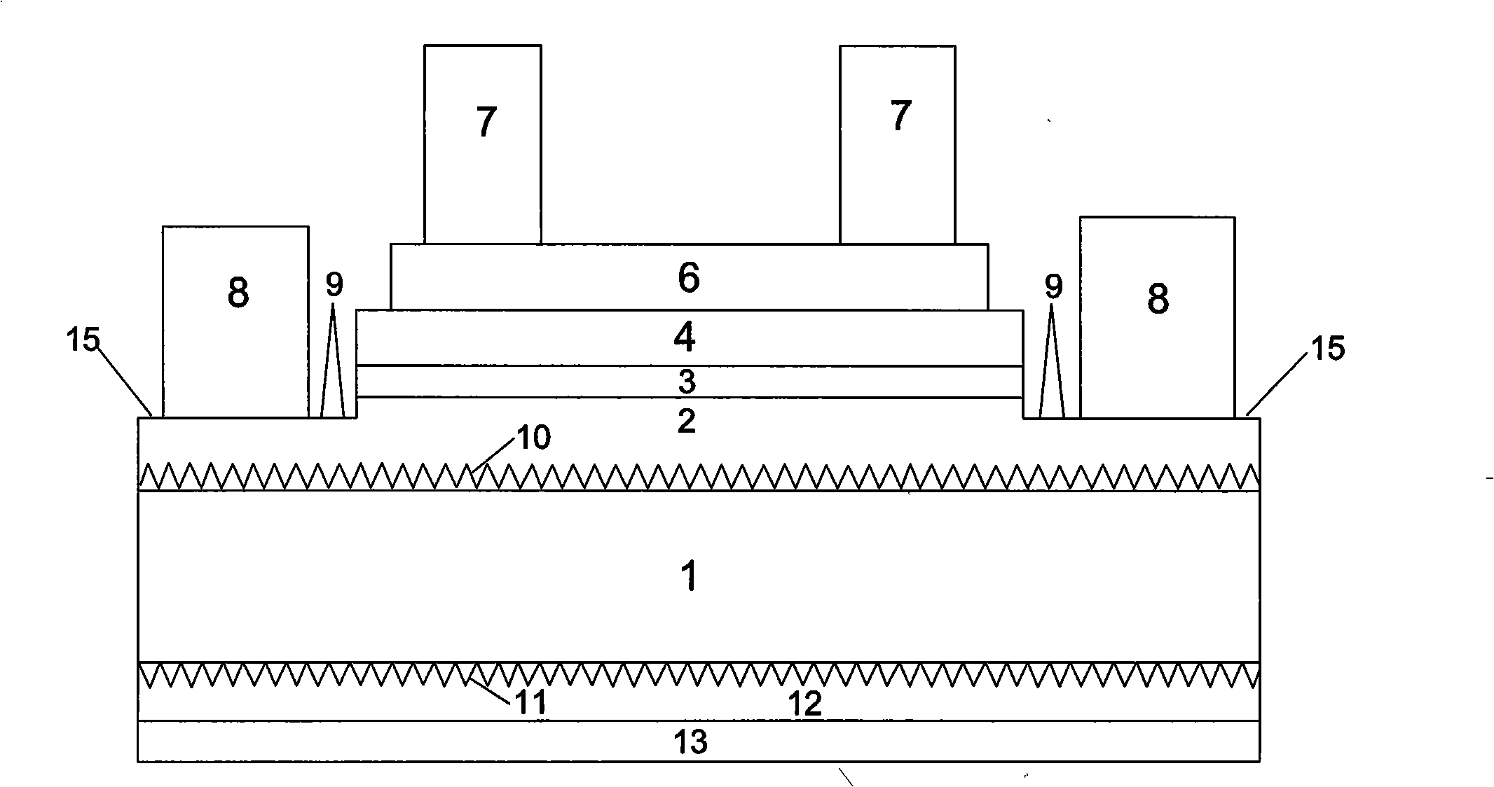
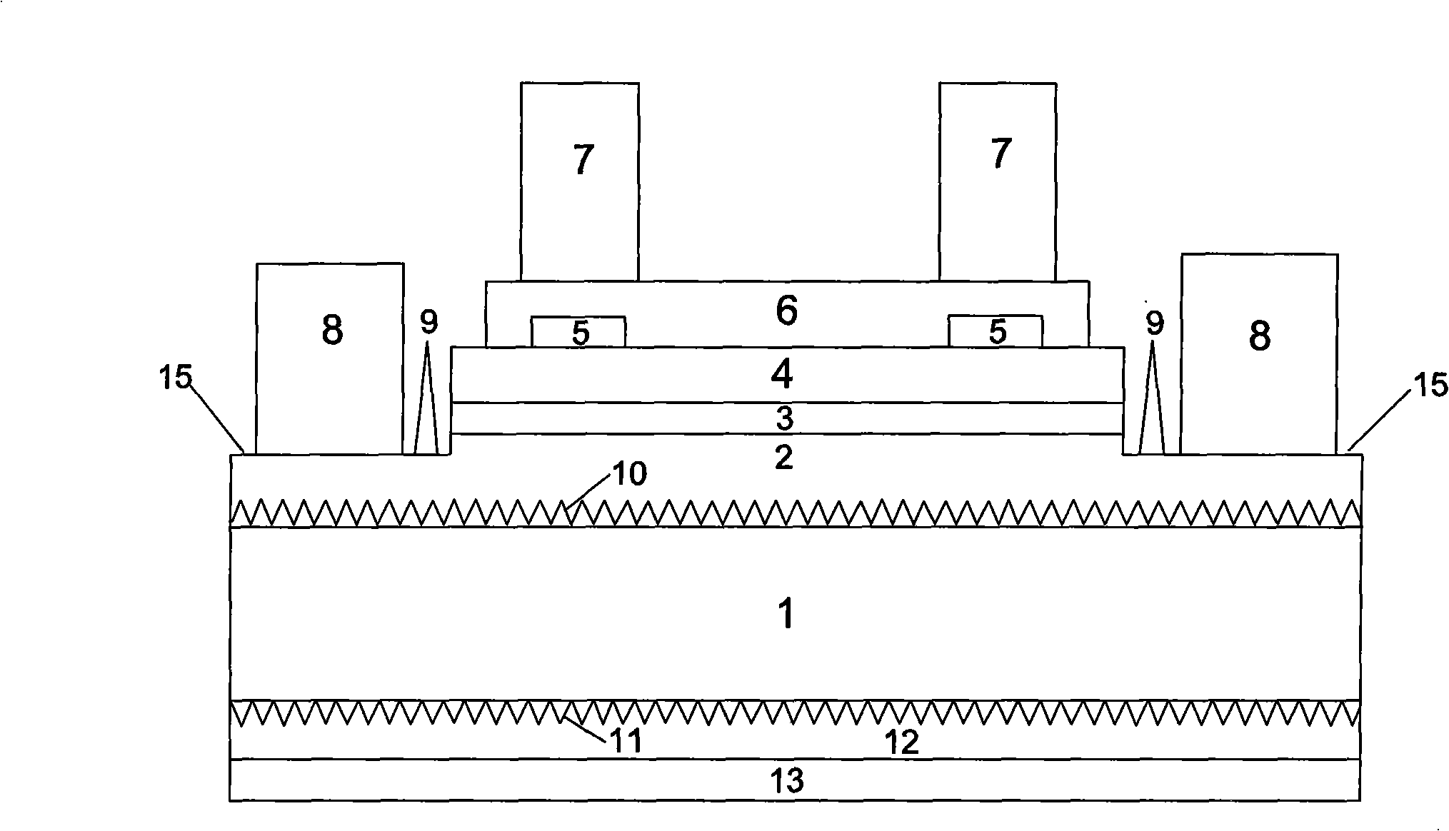
[0038] The first specific example is figure 1 and Figure 5As shown, the light-emitting diode chip of the present invention includes a substrate 1, an n-type semiconductor layer 2 formed on the front surface of the substrate 1, a light-emitting layer 3 formed on the n-type semiconductor layer 2, and a p-type semiconductor layer formed on the light-emitting layer 3. The semiconductor layer 4, the negative electrode bonding wire region 15 formed by etching on the n-type semiconductor layer 2, the positive electrode metal layer 7 formed on the p-type semiconductor layer 4, and the negative electrode metal layer formed on the negative electrode bonding wire region 15 layer 8, a conical optical microstructure 10 is provided on the front of the substrate 1, a conical optical microstructure 11 is provided on the back side of the substrate 1, a...


PUM

PropertyMeasurementUnit
heightaaaaaaaaaa
diameteraaaaaaaaaa
heightaaaaaaaaaa

Abstract

The invention discloses a surface coarsening LED chip and a manufacturing method thereof. A pyramidal optical microstructure is formed at the front of a substrate; an n type semiconductor layer, a luminous layer and a p type semiconductor layer are grown on the front of the etched substrate; a negative electrode weld line area is formed by etching, a negative electrode metal layer is manufactured on the negative electrode weld line area, a positive electrode metal layer is manufactured on the p type semiconductor layer; the pyramidal optical microstructure is formed at the local negative electrode weld line area among the negative electrode metal layer and the luminous layer and the p type semiconductor layer; burnishing by abrasion is carried out on the back of the substrate, then the pyramidal optical microstructure is formed on the back thereof. The pyramidal optical microstructure of the invention can reduce times of the total reflection of light and prevent part of light being absorbed by chips through the total reflection, thus facilitating the light emitted from the chips to be refracted to the outer surface of the chips at the highest speed with the greatest possibility, avoiding visible light resonance of the light inside the chips and improving light-emitting efficiency of the chips of the LED.

Description

【Technical field】 [0001] The invention relates to a chip, in particular to a roughened light-emitting diode chip. [0002] The invention also relates to a method for manufacturing a chip, in particular to a method for manufacturing a light-emitting diode chip with a roughened surface. 【Background technique】 [0003] The so-called light-emitting diode (Light-Emitting Diode) is a P / N diode made of a semiconductor material with a direct energy gap. Under the condition of thermal equilibrium, most of the electrons do not have enough energy to jump to the conduction band. Then apply a forward pressure, the electrons will jump to the conduction band, and the original position of the electrons on the original price bond band will generate holes. Under the appropriate general pressure, electrons and holes will combine in the P / N interface area (P-N Juction) to emit light, and the current of the power supply will continuously replenish electrons and holes to the N-type semiconductor...

Claims


Application Information

Patent Timeline
Patent Type & Authority Applications(China)
IPC IPC(8): H01L33/00
Inventor 樊邦扬叶国光梁伏波
Owner HE SHAN LIDE ELECTRONICS ENTERPRISE CO LTD
Why Eureka
Try Eureka