Photosensor
A light sensor, photoelectric conversion technology, applied in photovoltaic power generation, electric solid state devices, semiconductor devices, etc., can solve the problem of impossible to ensure photosensitivity
- Summary
- Abstract
- Description
- Claims
- Application Information
AI Technical Summary
Problems solved by technology
Method used
Image

Examples
no. 1 example
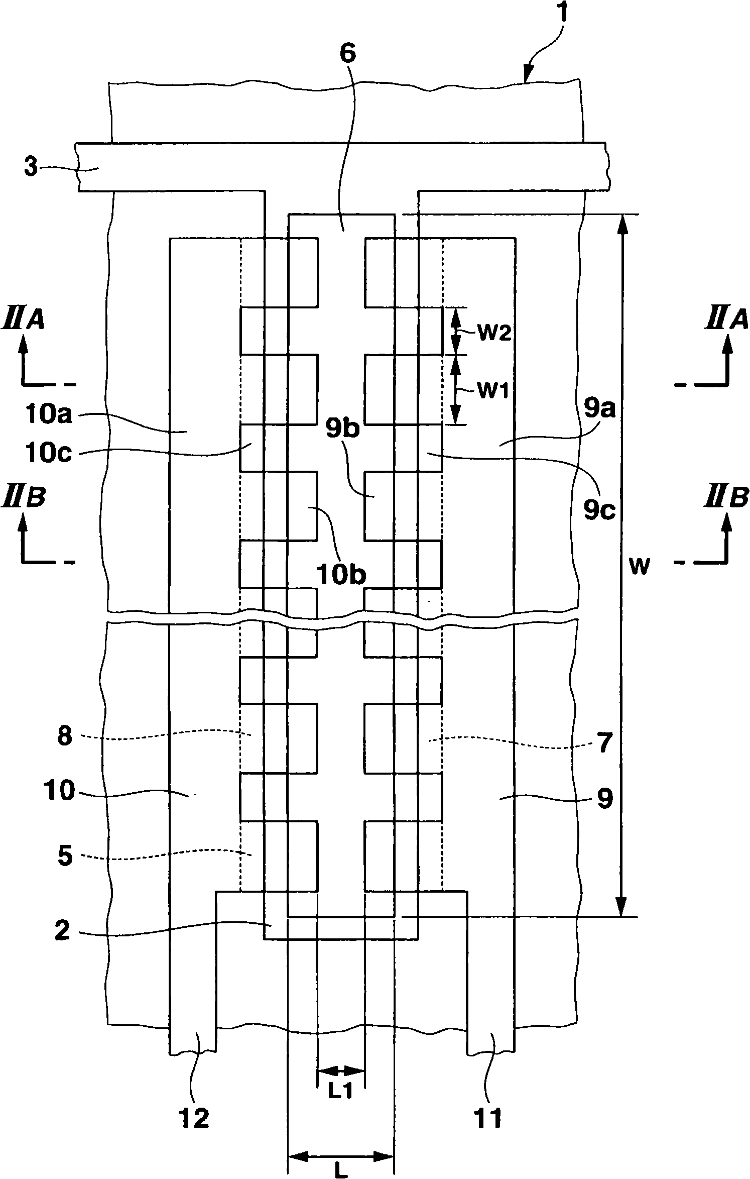
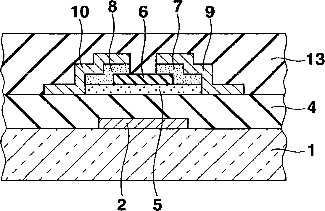
[0024] Figure 1-4 The structure of the first embodiment of the present invention is shown. figure 1 is a perspective plan view of the photosensor according to the first embodiment of the present invention. Figure 2A is along figure 1 The "II A -II A "A cross-sectional view taken along the line. Figure 2B is along figure 1 The "II B -II B "A cross-sectional view taken along the line.
[0025] The photosensor according to the first embodiment includes a substrate 1 made of glass or the like. Strip-shaped gate electrodes 2 made of chrome or the like and gate lines 3 connected to gate electrodes 2 are provided on the upper surface of substrate 1 .
[0026] On the upper surface of the substrate 1 is provided a gate insulating film 4 made of silicon nitride or the like, which covers the gate electrode 2 and the gate line 3 . A semiconductor thin film 5 for photoelectric conversion composed of intrinsic amorphous silicon is provided on the upper surface of the gate insul...
no. 2 example
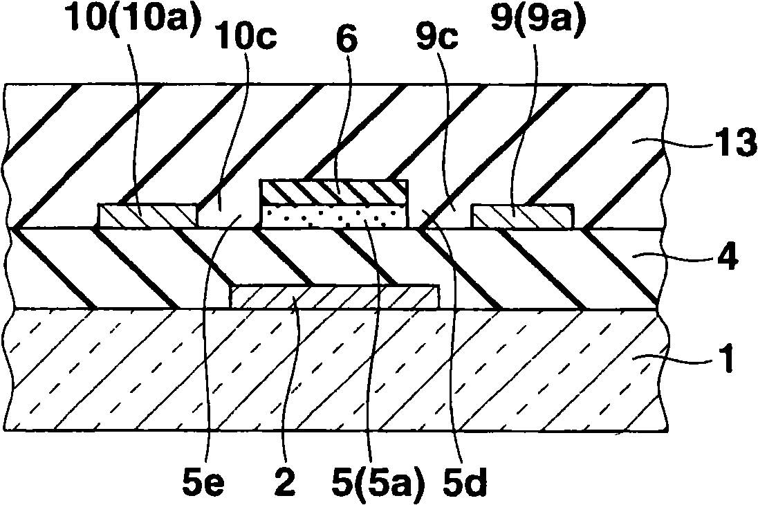
[0046] Figure 8-11 The structure of the second embodiment of the present invention is shown. Figure 8 is a perspective plan view of a light sensor according to a second embodiment of the present invention. Figure 9A is along Figure 8 IX A -IX A Cross-sectional view taken by line. Figure 9B is along Figure 8 IX B -IX B Cross-sectional view taken by line. Figure 10 yes Figure 8 , 9A and 9B are plan views of semiconductor thin films for photoelectric conversion. Figure 11 yes Figure 8 , 9A and the plan view of the ohmic contact layer shown in 9B.
[0047] The same elements as those described above with reference to the first embodiment are denoted by the same reference numerals. Reference numerals of structural elements in the second embodiment that are different from the corresponding elements in the first embodiment are designated with "'".
[0048] According to the photosensor of the second embodiment and Figure 1 to Figure 4 The photosensor accordin...
no. 3 example
[0054] Figure 12-15 The structure of the third embodiment of the present invention is shown. Figure 12 is a perspective plan view of a light sensor according to a third embodiment of the present invention. Figure 13A is along Figure 12 XIII A -XIII A Cross-sectional view taken by line. Figure 13B is along Figure 12 XIII B -XIII B Cross-sectional view taken by line. Figure 14 yes Figure 12 , 13A and 13B are plan views of semiconductor thin films for photoelectric conversion. Figure 15 yes Figure 12 , 13A and a plan view of the ohmic contact layer shown in 13B.
PUM
 Abstract
Description
Claims
Application Information
 - R&D
- Intellectual Property
- Life Sciences
- Materials
- Tech Scout
- Unparalleled Data Quality
- Higher Quality Content
- 60% Fewer Hallucinations
Browse by: Latest US Patents, China's latest patents, Technical Efficacy Thesaurus, Application Domain, Technology Topic, Popular Technical Reports.
© 2025 PatSnap. All rights reserved.Legal|Privacy policy|Modern Slavery Act Transparency Statement|Sitemap|About US| Contact US: help@patsnap.com