Method and system for non-destructive distribution profiling of an element in a film
A thin film and element technology, applied in interference spectroscopy, spectrum investigation, etc., can solve the problem of not providing fast analysis of thin films
- Summary
- Abstract
- Description
- Claims
- Application Information
AI Technical Summary
Problems solved by technology
Method used
Image
Examples
Embodiment Construction
[0047] Example implementations have been described with reference to specific configurations and techniques. Those of ordinary skill in the art will understand various changes and modifications that may be made within the scope of the appended claims. In addition, known components, devices, components, circuits, process steps, etc. have not been listed in detail.
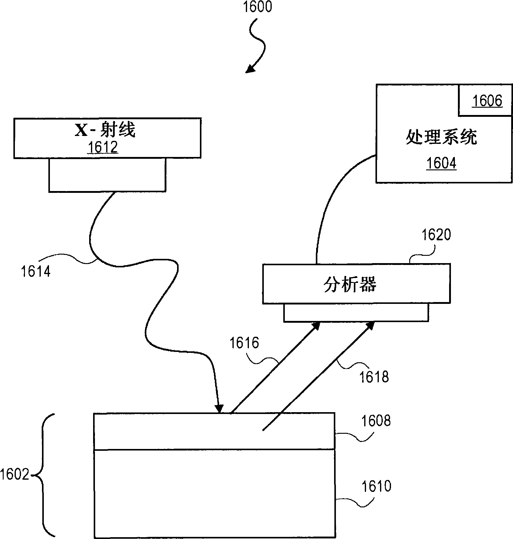
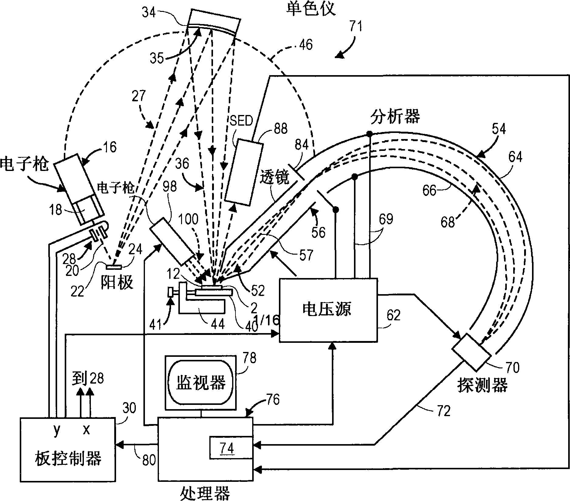
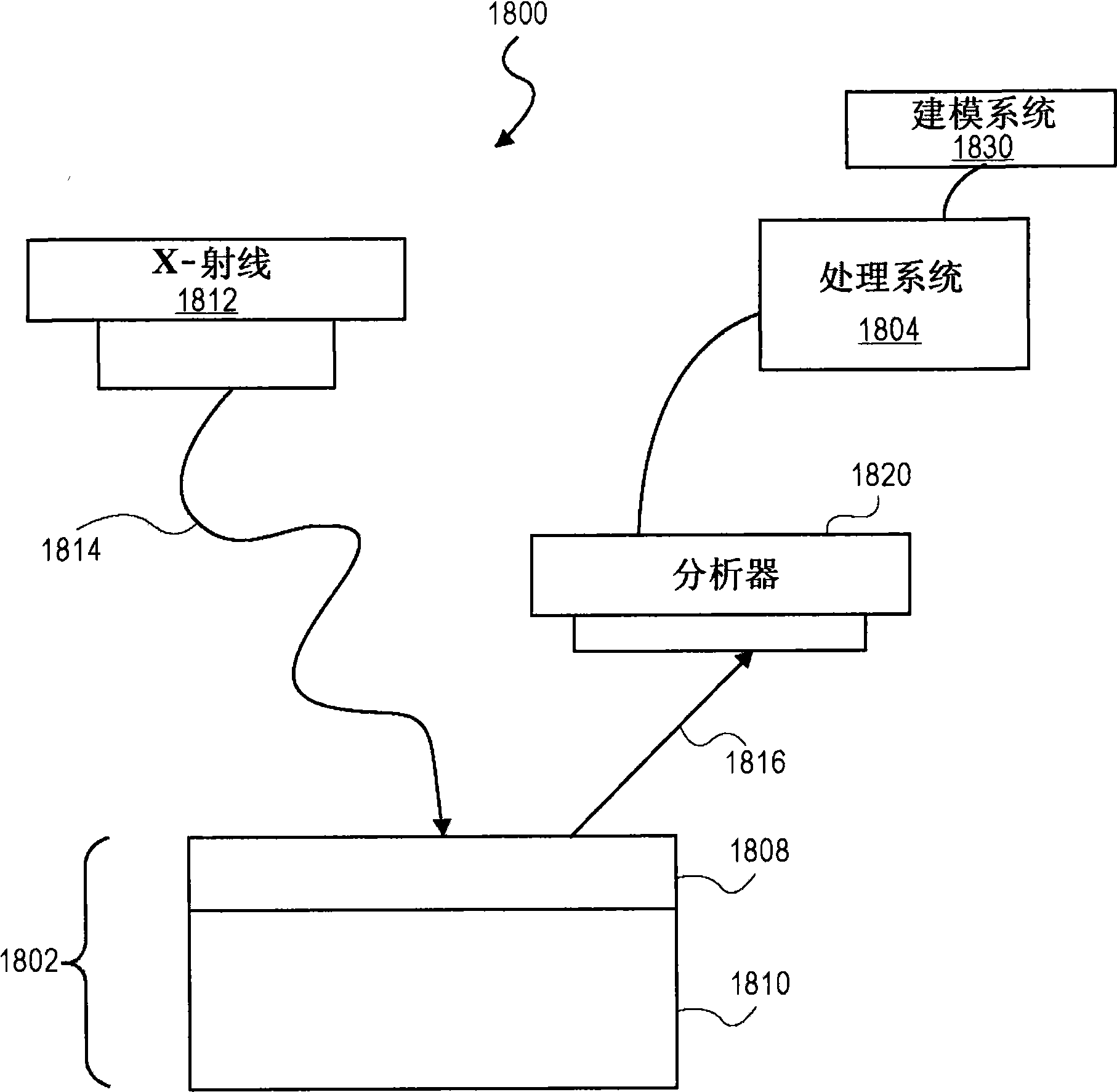
[0048] Embodiments of the present invention relate to a method and system for extracting depth distribution information and / or centroid values of one or more elements deposited in thin films or ultrathin films. The film thickness of the thin film is less than 20nm, in most cases less than 10nm, even less than 2nm. It is contemplated that embodiments of the present invention are similarly applicable to the analysis of thin films having a thickness greater than or equal to about 20 nm. In one main aspect of the invention, the depth distribution profile of an element in a thin film is determined. First, one or mor...
PUM
 Abstract
Description
Claims
Application Information


