Molecular electronic device fabrication methods and structures
A device structure and technology of electronic devices, applied in the direction of electric solid devices, electrical components, semiconductor devices, etc., to achieve the effect of eliminating short circuits
- Summary
- Abstract
- Description
- Claims
- Application Information
AI Technical Summary
Problems solved by technology
Method used
Image
Examples
Embodiment Construction
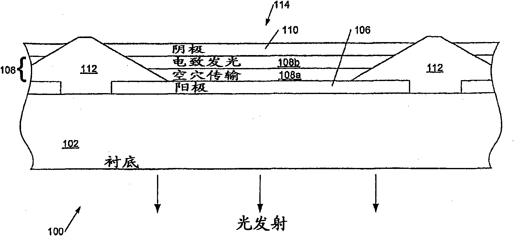
[0060] now refer to Figure 5 , which shows a well bounded on either side by banks that has been filled with a total ink volume V 1 until it overflows above the top of the well (can be measured by microscope). The banks in this figure have a height of about 1.5 μm, are flat on top and are shared by adjacent wells, and have a spacing of x b2 Separates two adjacent ink volumes in adjacent wells. The solution forms a contact angle with the bank material of approximately 35°; this is the angle formed by the surface of the dissolved material and the bank material it contacts. The tapered edge of the bank forms a similar bank angle, eg about 40°, with the plane of the substrate. The dotted lines in this figure represent the contours of the solutions in adjacent wells; it can be seen that careful control of the solution volume is required to avoid the spacing x b2 Reduced to the point where adjacent solutions merge.
[0061] Figure 6 shows that once the solvent has evaporated ...
PUM
 Abstract
Description
Claims
Application Information


