Thin quad flat no-lead package method

A flat leadless, packaging method technology, which is applied in the manufacture of electrical components, electrical solid devices, semiconductor/solid devices, etc., can solve the problems of device thickness restrictions, increase packaging manufacturing costs, restrictions, etc., and achieve thin device thickness and improved The effect of cooling efficiency

Active Publication Date: 2009-09-16
SHANGHAI KAIHONG ELECTRONICS CO LTD
View PDF0 Cites 3 Cited by
  • Summary
  • Abstract
  • Description
  • Claims
  • Application Information

AI Technical Summary

Problems solved by technology

Not only does this approach have limitations on the thickness of the device, but additional process steps may be introduced during implementation, and these additional process steps may become a source of potential process de

Method used


Image

  • Thin quad flat no-lead package method
  • Thin quad flat no-lead package method
  • Thin quad flat no-lead package method

Examples


Embodiment Construction

[0027] The specific implementation of the thin four-sided flat no-lead packaging method according to the present invention will be described in detail below in conjunction with the accompanying drawings.

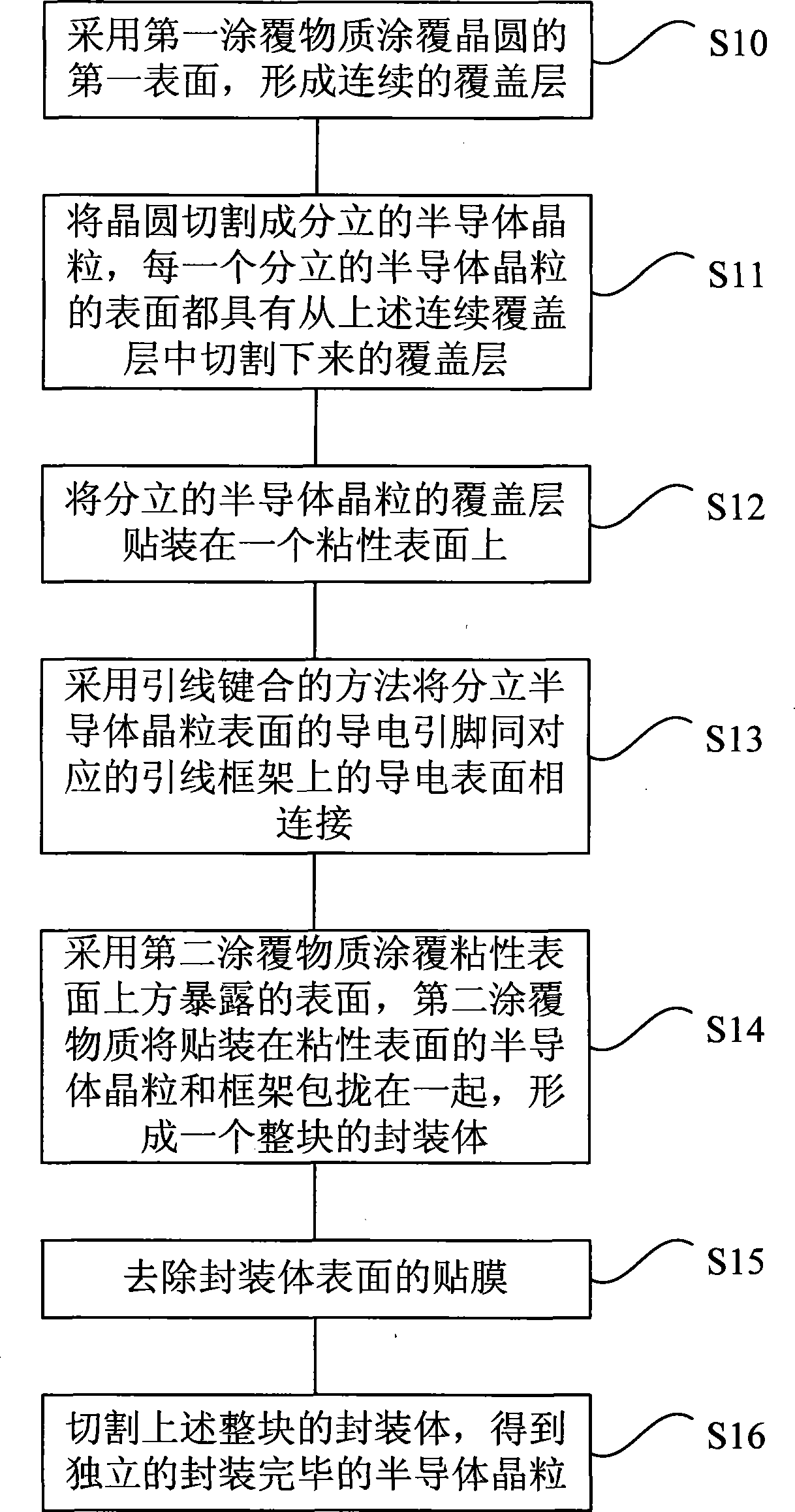
[0028] attached figure 1 Shown is a process flow chart of a specific embodiment of the thin four-sided flat no-lead packaging method described in the present invention. In step S10, the first surface of the wafer is coated with a first coating substance to form a continuous covering layer; in step S11, the wafer is cut into discrete semiconductor crystal grains, and the surface of each discrete semiconductor crystal grain has from The covering layer cut off from the above-mentioned continuous covering layer; step S12, attaching the covering layer of discrete semiconductor crystal grains on an adhesive surface; step S13, adopting the method of wire bonding to separate the conductive contacts on the surface of semiconductor crystal grains Connect with the conductive pins on t...


PUM


Abstract

A thin quad flat no-lead (QFN) package method comprises the following steps of: adopting a first coating substance (plastic package material) to be coated on a first surface (the back) of a wafer and form a continuous covering layer; cutting the wafer into a plurality of discrete semiconductor crystalline grains, each of which has the covering layer cut down from the continuous covering layer on the surface; mounting the covering layers of the plurality of discrete semiconductor crystalline grains on the surface of an adhesive film on a frame; after wire welding (lead bonding), adopting a second coating substance (plastic package material) to be coated on an exposed surface above an adhesive surface, and the second coating substance wraps together the semiconductor crystalline grains mounted on the adhesive surface to form a whole block of plastic package body; and cutting the whole block of plastic package body and obtaining a plurality of discrete completely packaged semiconductor crystalline grains (devices with complete functions). With the advantage that all the package processes have no special requirement on the structure of packaged chips, therefore the package method has universality, and besides, the device obtained by using the package method is very thin, thus being beneficial to improving the heat dissipation efficiency of chips.

Description

【Technical field】 [0001] The invention relates to the field of semiconductor packaging, in particular to a thin four-side flat no-lead packaging method. 【Background technique】 [0002] In everyday life, consumers demand more and more reliability, size, and price from products such as personal phones, personal digital assistants, and music players. For example, consumers want their personal phones to be ultra-thin and reliable. This requires packaged devices to be smaller and have fewer defects. In addition, these small form factor requirements may also require electronic components that dissipate heat from the packaging structure. [0003] Quad flat no lead package is a common packaging method in the prior art. The method is a standard packaging method using one lead frame and one die. This method not only has restrictions on the thickness of the device, but also may introduce additional process steps during implementation. These additional process steps may become a sou...

Claims


Application Information

Patent Timeline
IPC IPC(8): H01L21/50H01L21/56H01L21/78H01L21/60
CPCH01L2924/15153H01L2924/01082H01L23/3121H01L2224/97H01L2924/1517H01L29/0657H01L2224/83H01L2224/48091H01L2924/01013H01L2924/01003H01L2924/18301H01L24/97H01L2224/85H01L2224/274H01L24/27H01L24/85H01L2924/10158H01L2924/04953H01L24/48H01L2224/48247H01L21/6835H01L24/83H01L2221/68359H01L2924/18165H01L2924/01075H01L2224/73265H01L21/58H01L21/561H01L2924/00014H01L2924/181H01L2924/00012H01L2224/45099H01L2224/45015H01L2924/207
Inventor 谭小春李志宁蒋晓兰
Owner SHANGHAI KAIHONG ELECTRONICS CO LTD
Why Eureka
Try Eureka