Manufacturing method of flexible circuit board

A flexible circuit board and a manufacturing method technology, applied in the photoengraving process of the pattern surface, the removal of conductive materials by chemical/electrolytic methods, instruments, etc., can solve the problems of dry film plugging and other problems, so as to solve the problem of dry film plugging. Effect

Inactive Publication Date: 2009-09-16
苏州相城埭辰科技产业发展有限公司
View PDF1 Cites 8 Cited by
  • Summary
  • Abstract
  • Description
  • Claims
  • Application Information

AI Technical Summary

Problems solved by technology

[0010] The purpose of the present invention is to overcome the shortcoming that dry film plugging easily occurs in the preparation process of the prior art high-density flexible circuit board, and to provide a method for preparing a high-density flexible circuit board that can solve the problem of dry film plugging

Method used


Image

  • Manufacturing method of flexible circuit board
  • Manufacturing method of flexible circuit board
  • Manufacturing method of flexible circuit board

Examples


Embodiment 1

[0047] This embodiment is used to illustrate the preparation method of the flexible circuit board of the present invention.

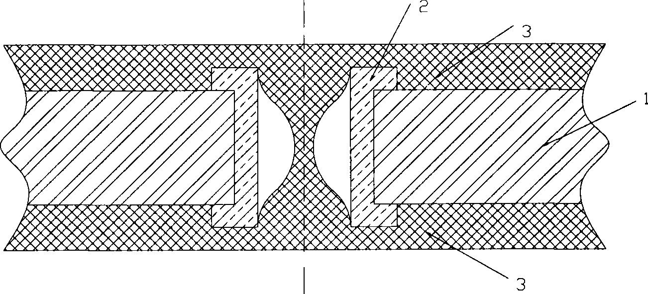
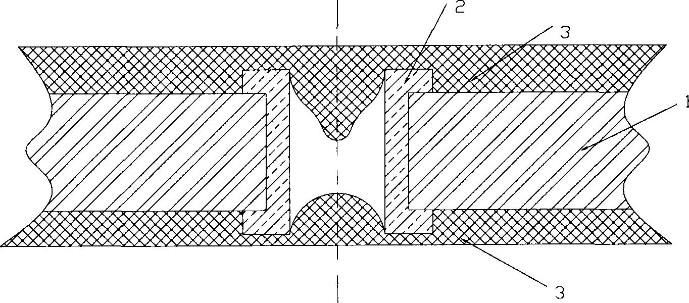
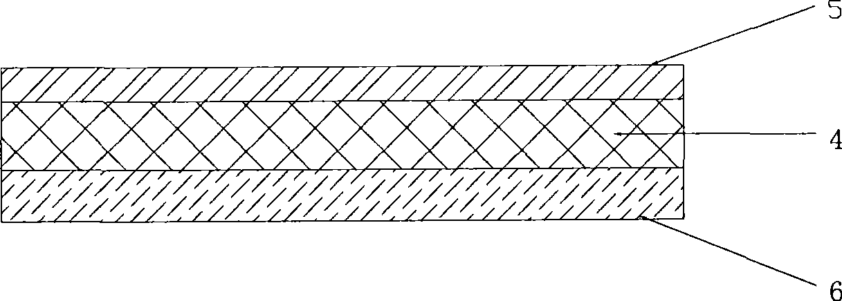
[0048] The structure of the selected copper clad laminate is as follows: Figure 4 As shown, among them, the materials of L1 and L2 surfaces are SL-12-12-EP of LG Company, and the material of prepreg is BH-10 of Taihong Company.

[0049] Laminate YQ-40SD dry film (thickness: 40 microns) on the L1 surface, laminate AQ-20FA dry film (thickness: 20 microns) on the L2 surface; paste the negative film (Shenzhen Meike Silver Co., Ltd.) on the L1 surface with a thick dry film salt film) and exposed in a graphic manner with a 5 kW high-pressure mercury lamp, the L2 surface is directly exposed, and the exposure energy of the L1 surface is 50 mJ / cm2, and the exposure energy of the L2 surface is 30 mJ / cm2; the L1 surface Tear off polyester film; at 30°C with 1.0 wt% Na 2 CO 3 The solution was used to develop the L1 and L2 surfaces; at 48°C, with CuCl 2 / H 2 o...

Embodiment 2

[0052] This embodiment is used to illustrate the preparation method of the flexible circuit board of the present invention.

[0053] According to the same method as in Example 1, the difference is that the thickness of the dry film used is respectively: the thick dry film is 40 microns (YQ-40SD), and the thin dry film is 15 microns (SPG-152).

[0054] Prepare 400 sheets of the same flexible circuit board by the above method, and the product is marked as A2.

Embodiment 3

[0056] This embodiment is used to illustrate the preparation method of the flexible circuit board of the present invention.

[0057] According to the same method as in Example 1, the difference is that the thicknesses of the dry films used are: the thick dry film is 50 microns (YQ-50SD), and the thin dry film is 20 microns (AQ-20FA).

[0058] Prepare 400 sheets of the same flexible circuit board by the above method, and the product is marked as A3.


PUM


Abstract

The invention provides a manufacturing method of flexible circuit board, which changes the double-sided thick photosensitive layer in the prior art into the layer with a thick photosensitive layer on one side and a thin photosensitive layer on the other side. Moreover, the method of respectively forming the two sides is adopted, thereby completely preventing the linkage of the photosensitive layers in the through hole and solving the problem that the dry membrane blocks the hole during the manufacturing process of the high-density flexible printed circuit board.

Description

technical field [0001] The invention relates to a manufacturing method of a flexible circuit board. Background technique [0002] Flexible Printed Circuit (FPC for short) is a printed circuit made of polyimide or polyester film-based copper clad laminate, which has high reliability and excellent flexibility. Due to its special functions, FPC is used more and more widely, and is becoming one of the most important products of copper clad laminates. [0003] The production process of the flexible printed circuit in the prior art is: on the two surfaces of the flexible double-sided copper clad laminate, the dry film including the photosensitive layer and the carrier layer is pressed; the negative film is pasted on the dry film on the two surfaces; After removing the carrier layer of the dry film on both surfaces, develop and etch; finally, peel off the photosensitive layer on both surfaces with a stripping solution. [0004] In recent years, flexible printed circuit boards hav...

Claims


Application Information

Patent Timeline
Patent Type & Authority Applications(China)
IPC IPC(8): H05K3/06G03F7/00
Inventor 韩垂华焦鑫
Owner 苏州相城埭辰科技产业发展有限公司
Why Eureka
Try Eureka