Manufacturing method of flexible circuit board
The technology of a flexible circuit board and a manufacturing method, which is applied in the direction of removing conductive materials by chemical/electrolytic methods, can solve problems such as dry film plugging, and achieve the effect of solving dry film plugging.
- Summary
- Abstract
- Description
- Claims
- Application Information
AI Technical Summary
Problems solved by technology
Method used
Image
Examples
Embodiment 1
[0047] This embodiment is used to illustrate the preparation method of the flexible circuit board of the present invention.
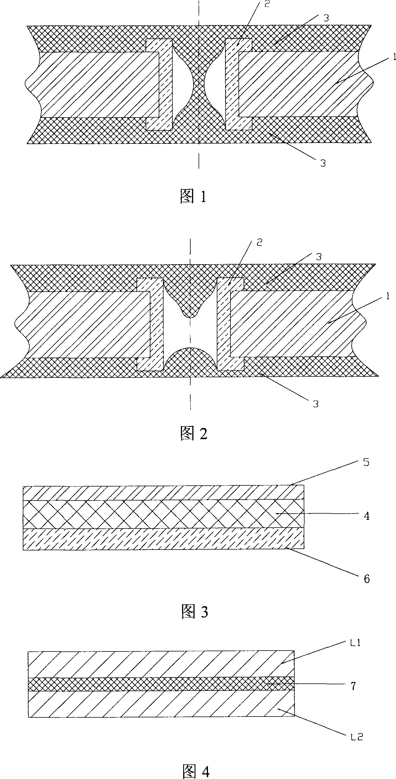
[0048] The structure of the selected copper-clad laminate is shown in Figure 4, in which the materials of the L1 and L2 surfaces are SL-12-12-EP of LG Company, and the material of the prepreg is BH-10 of Taihong Company.
[0049] Laminate YQ-40SD dry film (thickness: 40 microns) on the L1 surface, laminate AQ-20FA dry film (thickness: 20 microns) on the L2 surface; paste the negative film (Shenzhen Meike Silver Co., Ltd.) on the L1 surface with a thick dry film salt film) and exposed in a graphic manner with a 5 kW high-pressure mercury lamp, the L2 surface is directly exposed, and the exposure energy of the L1 surface is 50 mJ / cm2, and the exposure energy of the L2 surface is 30 mJ / cm2; the L1 surface Tear off polyester film; at 30°C with 1.0 wt% Na 2 CO 3 The solution was used to develop the L1 and L2 surfaces; at 48°C, with CuCl 2 / H 2 o 2 / HCl ...
Embodiment 2
[0052] This embodiment is used to illustrate the preparation method of the flexible circuit board of the present invention.
[0053] According to the same method as in Example 1, the difference is that the thickness of the dry film used is respectively: the thick dry film is 40 microns (YQ-40SD), and the thin dry film is 15 microns (SPG-152).
[0054] Prepare 400 sheets of the same flexible circuit board by the above method, and the product is marked as A2.
Embodiment 3
[0056] This embodiment is used to illustrate the preparation method of the flexible circuit board of the present invention.
[0057] According to the same method as in Example 1, the difference is that the thicknesses of the dry films used are: the thick dry film is 50 microns (YQ-50SD), and the thin dry film is 20 microns (AQ-20FA).
[0058] Prepare 400 sheets of the same flexible circuit board by the above method, and the product is marked as A3.
PUM
 Abstract
Description
Claims
Application Information

