

Organic EL device and manufacturing method thereof
A technology of electroluminescent devices and manufacturing methods, which is applied in the directions of organic semiconductor devices, semiconductor/solid-state device manufacturing, and electric solid-state devices, and can solve problems such as lowering yield, TFT and difficulty in driving TFT, etc., to achieve improved yield, reliable link effect
- Summary
- Abstract
- Description
- Claims
- Application Information
AI Technical Summary
Problems solved by technology
Method used
Image

Examples
Embodiment approach 1
[0102] In Embodiment 1, an organic EL device in which the switching TFT (element A) is a top-gate TFT and the driving TFT (element B) is a bottom-gate TFT will be described. In addition, the semiconductor layer in Embodiment 1 is a silicon-based semiconductor layer or a compound semiconductor layer.
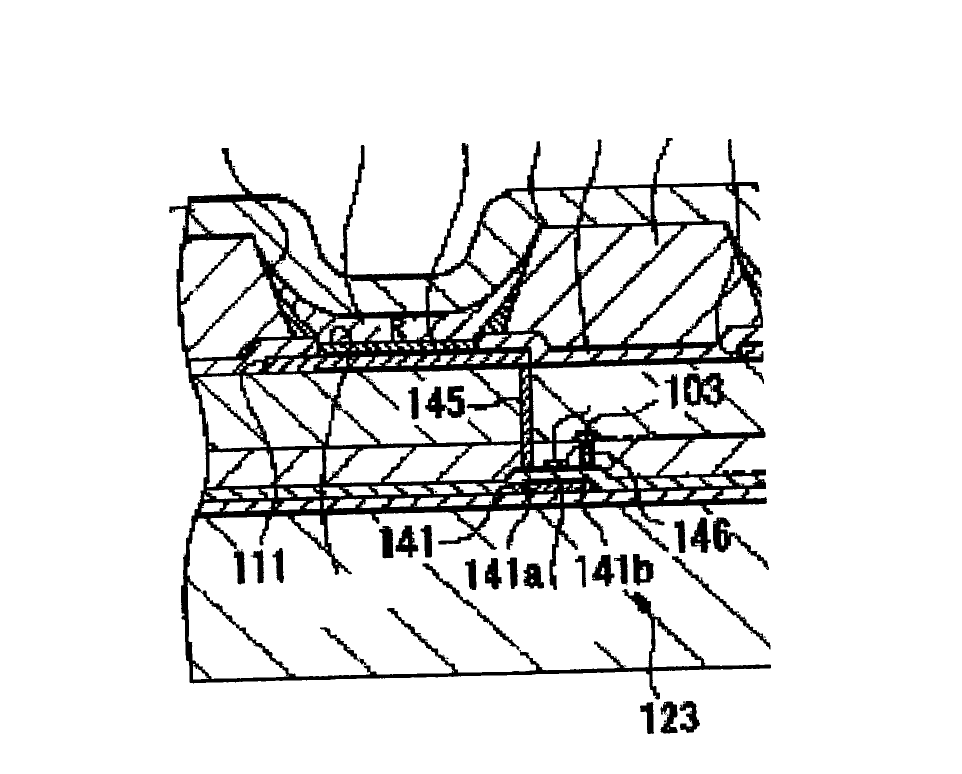
[0103] Figure 5 A cross-sectional view of the organic EL device according to Embodiment 1 is shown.
[0104] 1. About the organic EL device of Embodiment 1
[0105] exist Figure 5 Among them, the organic EL device 10 includes: a switching TFT 100 , a driving TFT 200 , and an organic EL element 300 .
[0106] The switching TFT 100 is a top-gate TFT. The switching TFT 100 includes a substrate 110 , a source electrode 120 and a drain electrode 121 , a semiconductor layer 130 , a gate insulating film 140 , and a gate electrode 122 .
[0107] In the top-gate switching TFT 100, the source electrode 120 and the drain electrode 121 are disposed on the substrate 110, the gate insul...
Embodiment approach 2
[0144] In Embodiment 1, an organic EL device in which the semiconductor is a silicon-based semiconductor layer or a compound semiconductor layer has been described. In Embodiment 2, an organic EL device in which the semiconductor layer is an organic semiconductor layer formed by a coating method will be described.
[0145] Figure 7 A cross-sectional view showing an organic EL device according to Embodiment 2. FIG.
[0146] 1. About the organic EL device of Embodiment 2
[0147] The organic EL device 20 of the second embodiment is the same as the organic EL device 10 of the first embodiment except for the semiconductor layer 131 of the switching TFT 101 , the semiconductor layer 231 of the driving TFT 201 , and the banks 160 and 260 . Components that are the same as those of the organic EL device 10 are assigned the same reference numerals, and description thereof will be omitted.
[0148] The switching TFT 101 has a bank 160 on the source electrode 120 and the drain electr...
Embodiment approach 3
[0177] In Embodiment 1 and Embodiment 2, an organic EL device in which the switching TFT is of the top gate type and the driving TFT is of the bottom gate type has been described. In Embodiment 3, an organic semiconductor device in which the switching TFT is a bottom-gate TFT and the driving TFT is a top-gate TFT will be described. In addition, in this embodiment mode, illustration of an organic EL element is omitted, and an organic semiconductor device will be described. Furthermore, the material of the semiconductor layer in this embodiment mode is an organic semiconductor.
[0178] 1. About the semiconductor device of the third embodiment
[0179] Figure 9 A cross-sectional view of a semiconductor device according to Embodiment 3 is shown.
[0180] In the description of the organic semiconductor device 30 according to Embodiment 3, the same reference numerals are assigned to the same components as those of the organic EL device 20 , and the description thereof will be o...
PUM
 Abstract
Description
Claims
Application Information