Light detecting device for imaging

A technology for detection devices and photodetectors, which is applied in radiation control devices, image communications, solid-state image signal generators, etc., can solve the problems of not reaching the size, etc., and achieve the realization of size, improvement of light utilization efficiency, and reduction of intervals Effect

Active Publication Date: 2009-09-30
SAMSUNG ELECTRONICS CO LTD
View PDF1 Cites 10 Cited by
  • Summary
  • Abstract
  • Description
  • Claims
  • Application Information

AI Technical Summary

Problems solved by technology

Therefore, when a prism is used for light splitting, it is necessary to set the distance between the prism and the light detection surface at least tens to hundreds of μm or more, and the actual size cannot be achieved in terms of trial production.

Method used


Image

  • Light detecting device for imaging
  • Light detecting device for imaging
  • Light detecting device for imaging

Examples


Embodiment Construction

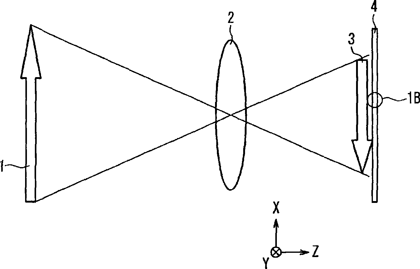
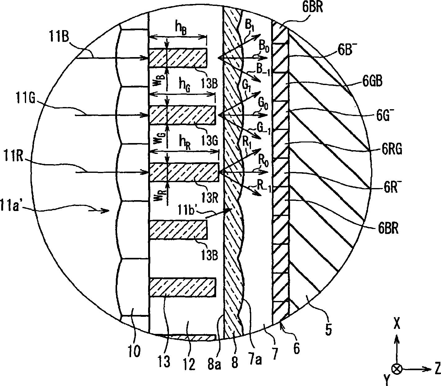
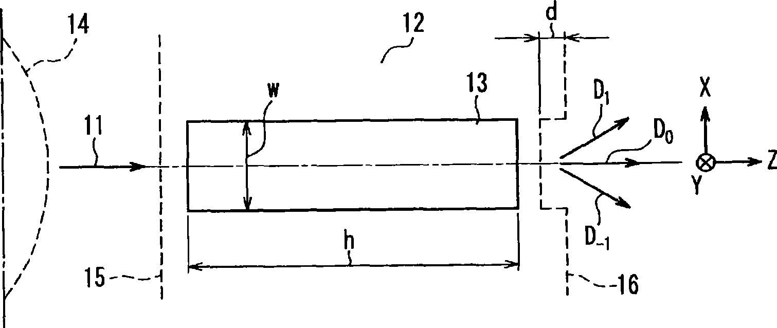
[0043] In the photodetection device for imaging of the present invention described above, it is preferable that the 0th-order diffracted light, the 1st-order diffracted light, and the −1st-order diffracted light are detected by the photodetectors that are different from each other. Accordingly, light having different wavelengths can be detected by different photodetectors.

[0044] In addition, preferably, the plurality of high-refractive-index transparent parts include at least red-standard high-refractive-index transparent parts, green-standard high-refractive-index transparent parts, and blue-standard high-refractive-index transparent parts that are different from each other in refractive index, shape, or size. department. In this case, it is preferable that, assuming that a, b, and c are integers equal to or greater than 0, the above-mentioned phase between light passing through the high-refractive-index transparent portion and light passing through the low-refractive-inde...


PUM


Abstract

A light detecting device for imaging comprises a plurality of light detectors (6) that are arranged on a substrate (5) one- or two-dimensionally, a low refractive index transparent layer (12) that is formed over the light detectors, and a plurality of high refractive index transparent portion (13) formed in a column-shape or a plate-like shape which are embedded in the low refractive index transparent layer along an arrangement direction of the light detectors. Two or more light detectors are arranged for one high refractive index transparent portion. When light inputted into the low refractive index transparent layer or the high refractive index transparent portion passes through these, a phase shift is caused in its wave surface and the light is separated into a 0-th order diffracted light, a 1st order diffracted light, and a -1st order diffracted light. Therefore, improvement of light use efficiency and a higher density of pixels can be realized.

Description

technical field [0001] The present invention relates to an imaging photodetection device used for imaging an image of an object. Background technique [0002] Conventional photodetection devices for imaging are disclosed in Non-Patent Document 1 and Non-Patent Document 2, for example. The outline of the photodetection device for imaging disclosed in these documents will be described below. [0003] Figure 9A It is a side view showing a schematic configuration of a conventional imaging device. Light such as natural light is incident on the object 1, and the reflected light passes through the lens system 2 to form an image 3 on a photodetector 4 such as CCD or CMOS. The lens system 2 is generally constructed by combining a plurality of lenses arranged along the optical axis in order to ensure optical performance. Figure 9A In simplified drawings, depicted as a single lens. [0004] Figure 9B is a drawing showing a schematic structure of the photodetection device 4, and ...

Claims


Application Information

Patent Timeline
Patent Type & Authority Applications(China)
IPC IPC(8): H01L27/14H04N5/335H01L27/148H04N5/369H04N5/372H04N5/374
CPCH01L27/14621H04N9/045H01L27/14627H01L27/14629H04N23/10H04N25/134
Inventor 西胁青儿
Owner SAMSUNG ELECTRONICS CO LTD
Why Eureka
Try Eureka