Sintering method and device for configurable firmware

A sintering method and firmware technology, applied in the communication field, can solve problems such as high error rate, failure, and affecting the normal operation of the system, so as to reduce failure and overcome the effect of high error rate

Inactive Publication Date: 2011-11-30
ZTE CORP
View PDF0 Cites 0 Cited by
  • Summary
  • Abstract
  • Description
  • Claims
  • Application Information

AI Technical Summary

Problems solved by technology

[0009] The present invention is proposed to solve the above-mentioned problem that curing the configurable firmware of a single board by manual sintering tools will lead to a high error rate, which will cause the system to fail during operation and affect the normal operation of the system.

Method used


Image

  • Sintering method and device for configurable firmware
  • Sintering method and device for configurable firmware
  • Sintering method and device for configurable firmware

Examples


Embodiment Construction

[0030] Functional Overview

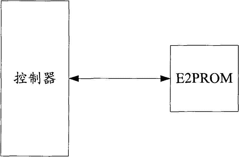
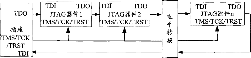
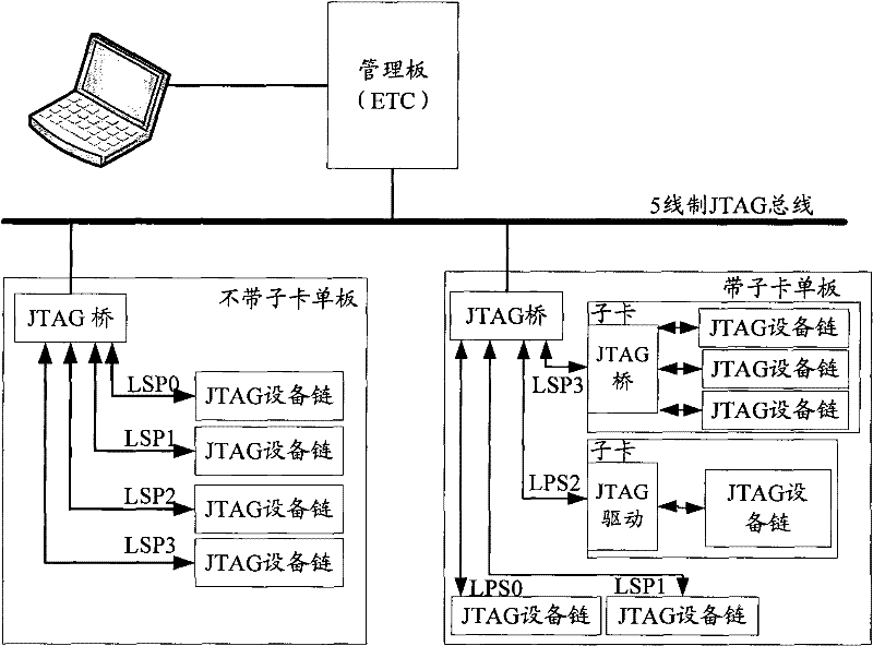
[0031] As mentioned above, in the prior art, manual sintering tools are used to solidify the configurable firmware of the single board, which leads to a high error rate, and then makes the system fail during operation, affecting the normal operation of the system. Based on this, the present invention combines configurable firmware and SJTAG to realize sintering of configurable firmware content. The basic idea of ​​the present invention is: the ETC scans the specific pin of the EPLD (Electrically Programmable Logic Device) of the single board to obtain the ID number of the single board, obtains the sub-chain information to be sintered according to the single board ID, and then, according to the The corresponding connection relationship between the device pins and the configurable firmware in the sub-chain information controls the BSC in the device pins, simulates the interface timing of the configurable firmware, and realizes the sintering of the co...


PUM


Abstract

The present invention provides a sintering method and device for configurable firmware, wherein the sintering method for configurable firmware includes: the test controller ETC obtains sub-chain information to be sintered according to the board identification ID of the device, wherein the sub-chain information is at least Including the corresponding connection relationship between device pins and configurable firmware; according to the sub-chain information, ETC controls the boundary scan unit BSC in the device pins to simulate the interface timing of configurable firmware, and realize the sintering of configurable firmware content according to the simulated interface timing . The present invention overcomes the problem in the prior art that the manual sintering tool solidifies the single-board configurable firmware will cause a relatively high error rate, thereby reducing system failures during operation.

Description

technical field [0001] The present invention relates to the communication field, in particular to a sintering method and device for configurable firmware. Background technique [0002] With the increase in the demand for single boards in communication equipment, the increase in the number of smart devices on the single board and their integration, and in order to cooperate with the start-up of the single board and the electronic identification of the single board, most of the single boards are equipped with I2C bus or SPI (Serial Peripheral Interface, Serial Peripheral Interface) bus non-volatile electrically erasable programmable read-only memory (Electrically Erasable Programmable Read-Only Memory, referred to as E2PROM). figure 1 It is a structural schematic block diagram of E2PROM and controller in the related art, such as figure 1 As shown, the E2PROM is used to record the startup information of the board and the configuration information of the board, for example, the...

Claims


Application Information

Patent Timeline
Patent Type & Authority Patents(China)
IPC IPC(8): G06F11/267G06F9/445
Inventor 张凯查卫民李孝军陈彬
Owner ZTE CORP
Why Eureka
Try Eureka