Synchronous voltage booster circuit with active negative current modulation and control method thereof

A synchronous boost and modulation circuit technology, applied in control/regulation systems, high-efficiency power electronic conversion, electrical components, etc., can solve problems affecting circuit performance, high-frequency ripple, reducing efficiency, etc., to maintain efficiency, suppress high Frequency oscillation, the effect of reducing EMI

Active Publication Date: 2013-04-10
CHENGDU MONOLITHIC POWER SYST
View PDF0 Cites 0 Cited by
  • Summary
  • Abstract
  • Description
  • Claims
  • Application Information

AI Technical Summary

Problems solved by technology

[0003] In addition, due to the influence of parasitic parameters, the turn-off of the high-side transistor will cause high-frequency oscillation at the switch node
Usually, the frequency of this oscillation is much higher than the switching frequency, so high-frequency ripples will appear at the output, causing electromagnetic interference (EMI) and affecting the performance of the entire circuit
Existing techniques typically use passive RC snubber circuits to suppress oscillations, which, while effective, can significantly reduce efficiency

Method used


Image

  • Synchronous voltage booster circuit with active negative current modulation and control method thereof
  • Synchronous voltage booster circuit with active negative current modulation and control method thereof
  • Synchronous voltage booster circuit with active negative current modulation and control method thereof

Examples


Embodiment Construction

[0014] Specific embodiments of the present invention will be described in detail below, and it should be noted that the embodiments described here are only for illustration, not for limiting the present invention.

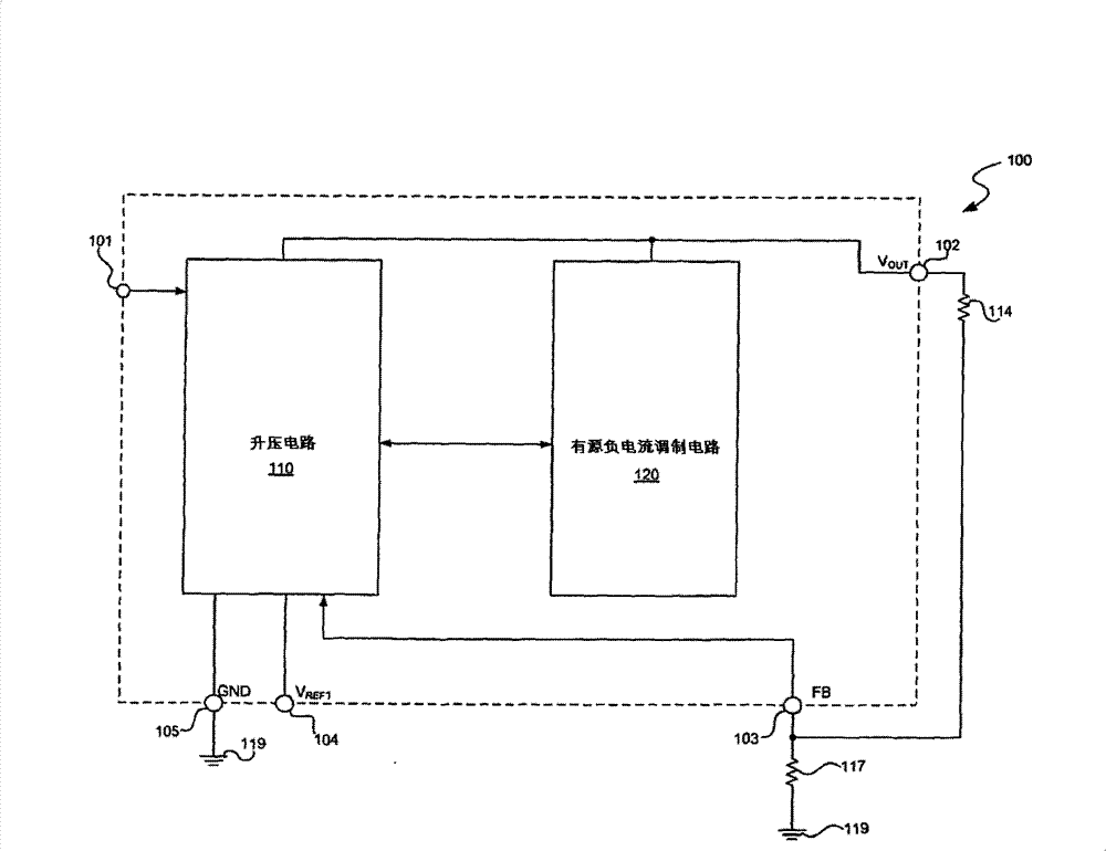
[0015] figure 1 It is a block diagram of a synchronous boost circuit 100 with active negative current modulation according to an embodiment of the present invention. The synchronous boost circuit 100 includes a boost circuit 110 and an active negative current modulation circuit 120 . In one embodiment, the synchronous boost circuit 100 may be an integrated circuit package, including a switch node pin 101 , an output pin 102 , a feedback pin 103 , a reference voltage pin 104 and a ground pin 105 . The output voltage V is available at the output pin 102 OUT , and the output voltage V OUT It is fed back here via the series connected resistor 114 and resistor 117 . The feedback voltage FB of the above two resistor connection terminals is connected to the feedback p...


PUM


Abstract

A switch-mode synchronous boost voltage regulator is disclosed that includes a boost voltage regulator and an active current modulator. The active current modulator detects a negative current flowing through the high-side switch during a light load condition. When the negative current is detected, the active current modulator is operable to maintain the high-side switch “on” in a linear mode and to limit the negative current to a predetermined current level.

Description

technical field [0001] The present invention relates to analog integrated circuits, and in particular, to a switch-mode voltage regulator circuit. Background technique [0002] In a traditional synchronous boost circuit, there are two switching transistors, which can be referred to as upper transistors or lower transistors respectively, and an inductor is connected to the input end thereof. Under low-load and no-load conditions, the conduction time of the upper transistor may be too long, causing the inductor current to drop to zero or even reverse, that is, the direction of the inductor current changes from positive to negative. Due to the voltage drop across the body diode of the LSB and the voltage overshoot caused by parasitic parameters, the reverse inductor current when entering and leaving the dead zone will generate additional voltage stress across the LSB. The greater the reverse inductor current, the greater the voltage stress. Therefore, it is necessary to limit...

Claims


Application Information

Patent Timeline
Patent Type & Authority Patents(China)
IPC IPC(8): G05F1/10
CPCY02B70/1466G05F1/56H02M3/1588H02M2001/0045H02M1/0045Y02B70/10
Inventor 詹姆斯·H·阮
Owner CHENGDU MONOLITHIC POWER SYST
Why Eureka
Try Eureka