Light-emitting diode and fabricating method thereof

A technology of light-emitting diodes and manufacturing methods, which is applied to electrical components, circuits, semiconductor devices, etc., and can solve problems such as difficulty in achieving long-distance lighting, increased lighting costs, and poor directivity

Inactive Publication Date: 2009-10-28
FU ZHUN PRECISION IND SHENZHEN +1
View PDF0 Cites 3 Cited by
  • Summary
  • Abstract
  • Description
  • Claims
  • Application Information

AI Technical Summary

Problems solved by technology

[0003] In actual use, because the light emitted by the LED is relatively scattered, it has poor directivity and affects the propagation distance of the light, so that the brightness of the light at a position farther away from the LED is low, and it is difficult to meet the needs of long-distance lighting. , the industry generally uses secondary optics to enhance the directivity of the light emitted by the LED. The usual method is to use the LED with a lens, such as using a convex lens or a Fresnel lens to generate a parallel beam, and the divergent light emitted by the LED Converted to substantially parallel rays to increase their travel distance
[0004] However, using this method requires an additional lens on one side of the LED, which increases the lighting cost of the LED

Method used


Image

  • Light-emitting diode and fabricating method thereof
  • Light-emitting diode and fabricating method thereof
  • Light-emitting diode and fabricating method thereof

Examples


Embodiment Construction

[0013] The present invention will be further described below in conjunction with the embodiments with reference to the accompanying drawings.

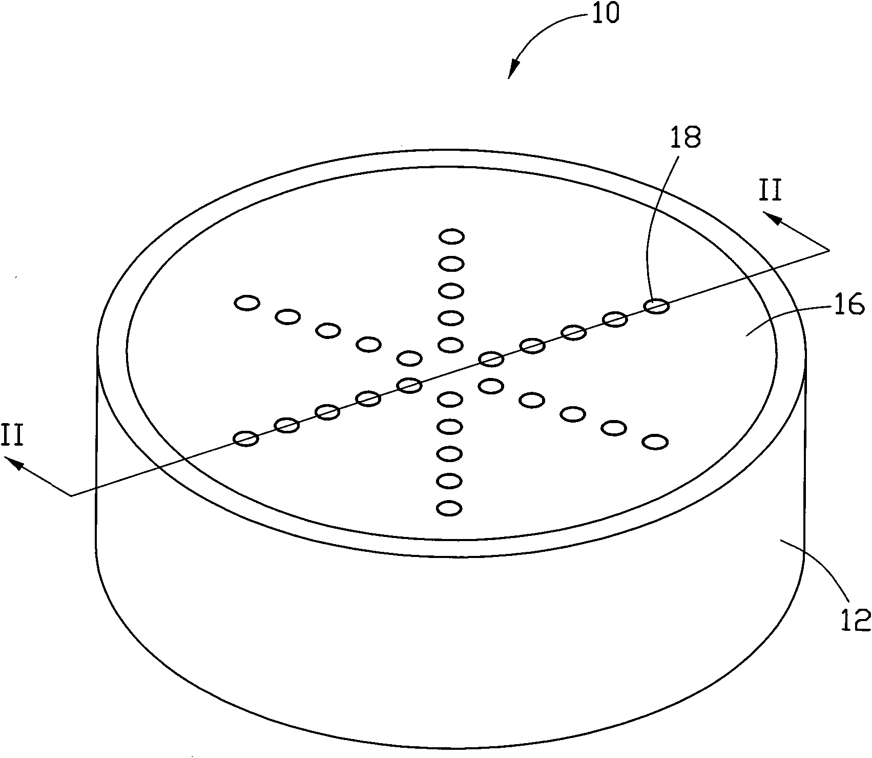
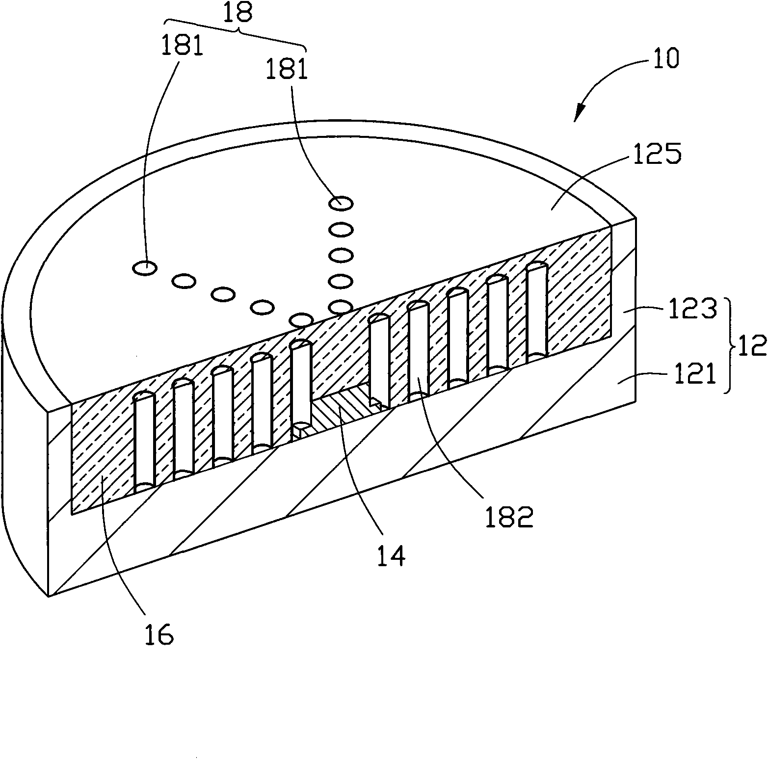
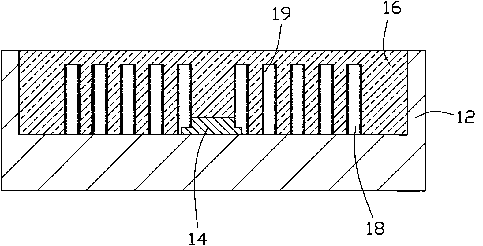
[0014] see figure 1 and figure 2 , the light emitting diode 10 of the present invention includes a base 12 , a light emitting chip 14 and a glue 16 .

[0015] The base 12 is made of conductive and thermally conductive metal and other materials, and includes a base plate 121 and a bowl cup 123 located above the base plate 121 . The substrate 121 is connected to an external power supply through pins. The bowl cup 123 is integrally formed with the base plate 121 , and forms a receiving cavity with the base plate 121 . The inner surface of the bowl cup 123 is a highly reflective surface to reflect the light incident on the sidewall of the bowl cup 123 to the light exit surface 125 located at the opening of the bowl cup 123 . In order to make the inner surface of the bowl 123 form a highly reflective surface, reflective layers such as ...


PUM


Abstract

The invention relates to a light-emitting diode which comprises a base plate, a luminescence chip, a cup and colloid, wherein the cup is positioned on the base plate, the colloid packages the luminescence chip into the cup, the colloid is internally provided with a plurality of holes, and the holes extend from the bottom of the colloid to the top of the colloid. The fabricating method of the light-emitting diode comprises the following steps: a first mould with a plurality of forming columns and a second mould with a hollow cavity are provided; the forming columns extend from the top of the first mould to the bottom of the first mould; the first mould is arranged into the hollow cavity of the second mould, and a certain distance exists between the bottom ends of the forming columns and the bottom of the hollow cavity; light transmittance materials are injected; the cooling is performed; the first mould and the second mould are removed, the colloid with the holes is formed, the upper end of each hole is opened and the lower end is closed; a base with the cup is provided, the luminescence chip is fixed into the cup of the base; the openings of the holes face down, the colloid is fixed into the cup of the base, and thus the light-emitting diode is fabricated.

Description

technical field [0001] The invention relates to an optical element and a manufacturing method thereof, in particular to a light emitting diode and a manufacturing method thereof. Background technique [0002] Light Emitting Diode (hereinafter referred to as LED) has been widely used in many occasions due to its advantages of small driving voltage, small size, low energy consumption, high brightness, fast response time, long life and environmental protection, such as as Signal light sources, traffic lights, car lights, electronic display boards, etc. [0003] In actual use, because the light emitted by the LED is relatively scattered, it has poor directivity and affects the propagation distance of the light, so that the brightness of the light at a position farther away from the LED is low, and it is difficult to meet the needs of long-distance lighting. , the industry generally uses secondary optics to enhance the directivity of the light emitted by the LED. The usual metho...

Claims


Application Information

Patent Timeline
Patent Type & Authority Applications(China)
IPC IPC(8): H01L33/00H01L33/54
CPCH01L33/54H01L2933/0091
Inventor 魏百盛张家寿
Owner FU ZHUN PRECISION IND SHENZHEN
Why Eureka
Try Eureka