Semiconductor device and method for fabricating the same

A semiconductor and device technology, applied in the field of semiconductor devices, can solve the problems of reducing the speed of word line signals, high resistance, etc.

Inactive Publication Date: 2009-11-04
SK HYNIX INC
View PDF1 Cites 3 Cited by
  • Summary
  • Abstract
  • Description
  • Claims
  • Application Information

AI Technical Summary

Problems solved by technology

However, since the surrounding gate includes a polysilicon layer, the voltage of the word line is transmitted through the structure, so the surrounding gate has a high resistance which reduces the signal speed of the word line

Method used


Image

  • Semiconductor device and method for fabricating the same
  • Semiconductor device and method for fabricating the same
  • Semiconductor device and method for fabricating the same

Examples


Embodiment Construction

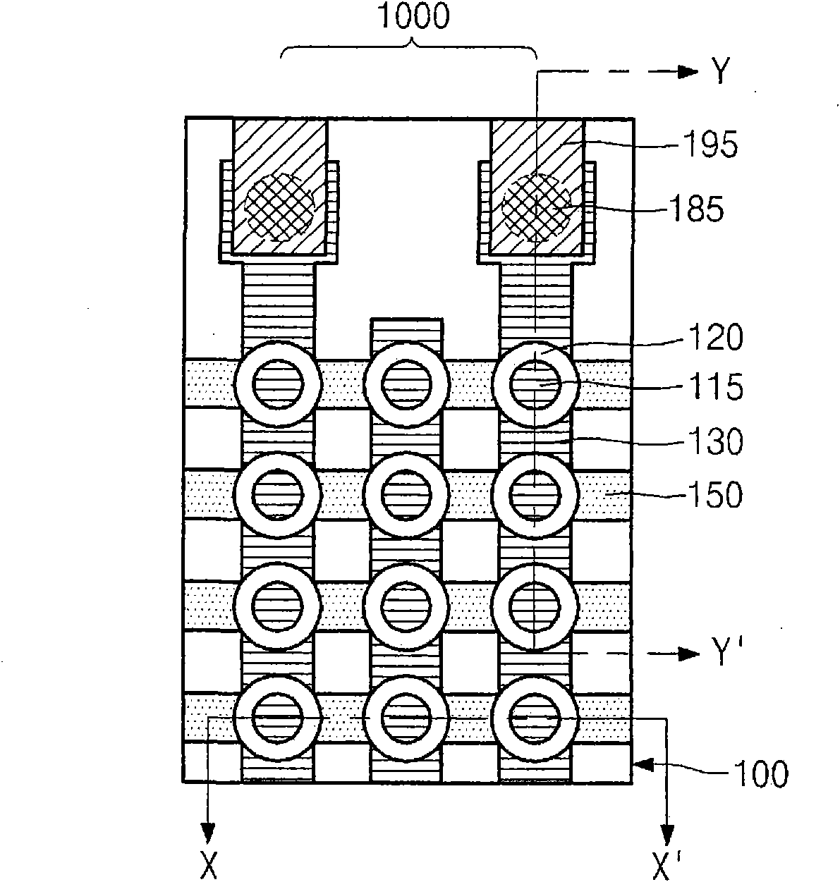
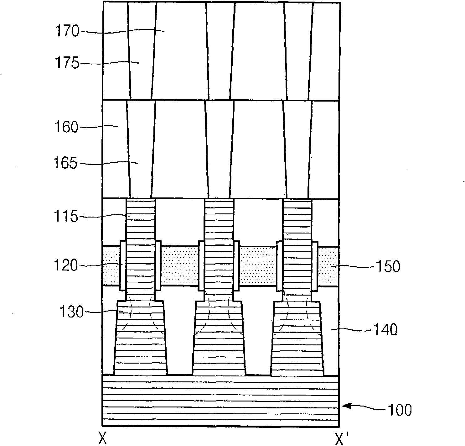
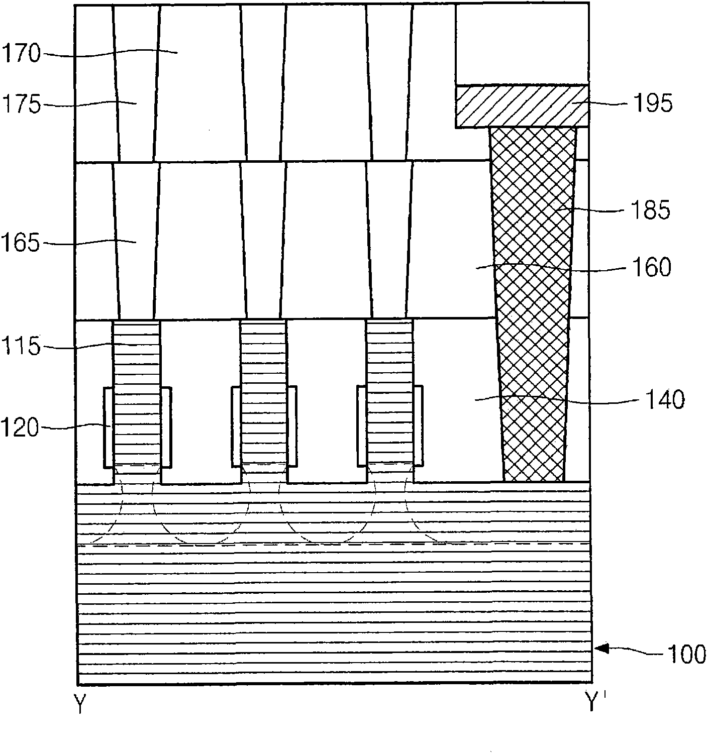
[0026] Figure 4 is a view showing a semiconductor device according to one embodiment of the present invention.

[0027] Figure 4 The semiconductor device includes a first word line 155 and a second word line 190, the first word line 155 is configured to electrically connect the surrounding gates of the vertical transistors together, the second word line 190 is arranged in parallel with the first word line above a word line, and is configured to supply a gate voltage to the first word line 155 . The second word line 190 is connected to the first word line 155 , and the first word line 155 is electrically connected to the second word line 190 through the contact plug 180 . The second word line 190 includes a metal line having good conductivity. The second word line 190 receives gate power from the peripheral circuit area, and supplies the gate power to the first word line 155 .

[0028] As shown, the gate voltages from the peripheral circuit regions are not applied directly ...


PUM


Abstract

The present invention discloses a semiconductor device and a mthod for fabricating the same. The method for fabricating a semiconductor device includes forming a metal word line additionally over a vertical transistor to obtain a multi-layered structure, thereby preventing degradation of the operating speed of the semiconductor device by preventing an increase of resistance of a damascene word line that connects a surrounding gate of a vertical transistor. As a result, the yield and reliability of the semiconductor device can be improved.

Description

technical field [0001] The present invention relates to a semiconductor device, and more particularly, to a structure and a manufacturing method of a semiconductor device for preventing a decrease in the operating speed of the semiconductor device. Background technique [0002] Semiconductor devices such as DRAM need to accommodate a large number of transistors in a limited area to increase integration. Therefore, a vertical transistor has been proposed for use as an element that typically has a 4F 2 Components included in a memory cell with a higher area of ​​integration. Vertical transistors have a wrap-around gate structure surrounding a vertical channel. [0003] For an area of ​​4F 2 A surrounding gate is formed in the region of the channel, and the channel region is selectively etched isotropically, so that the channel region is formed thinner than the source / drain region, thereby obtaining good device characteristics. Therefore, vertical transistors can effectivel...

Claims


Application Information

Patent Timeline
Patent Type & Authority Applications(China)
IPC IPC(8): H01L23/522H01L27/108H01L21/768H01L21/8242
CPCH01L29/7827H01L27/10876H01L27/10891H10B12/053H10B12/488H10B12/395H10B12/0383
Inventor 郑星雄黄祥珉金贤贞
Owner SK HYNIX INC
Why Eureka
Try Eureka