Reverting method of low dielectric materials and porous low-dielectric layer

A low-dielectric material, low-dielectric layer technology, applied in the manufacture of circuits, electrical components, semiconductor/solid-state devices, etc., can solve problems such as the increase in dielectric constant, prevent the operation speed from being reduced, and solve the problem of increasing the dielectric constant. Effect

Inactive Publication Date: 2007-04-25
UNITED MICROELECTRONICS CORP
View PDF0 Cites 4 Cited by
  • Summary
  • Abstract
  • Description
  • Claims
  • Application Information

AI Technical Summary

Problems solved by technology

[0006] Another object of the present invention is to provide a recovery method for a porous low-k layer to solve the problem of a rise in the dielectric constant of the porous low-k material due to the previous chemical mechanical polishing process

Method used


Image

  • Reverting method of low dielectric materials and porous low-dielectric layer
  • Reverting method of low dielectric materials and porous low-dielectric layer

Examples


Embodiment Construction

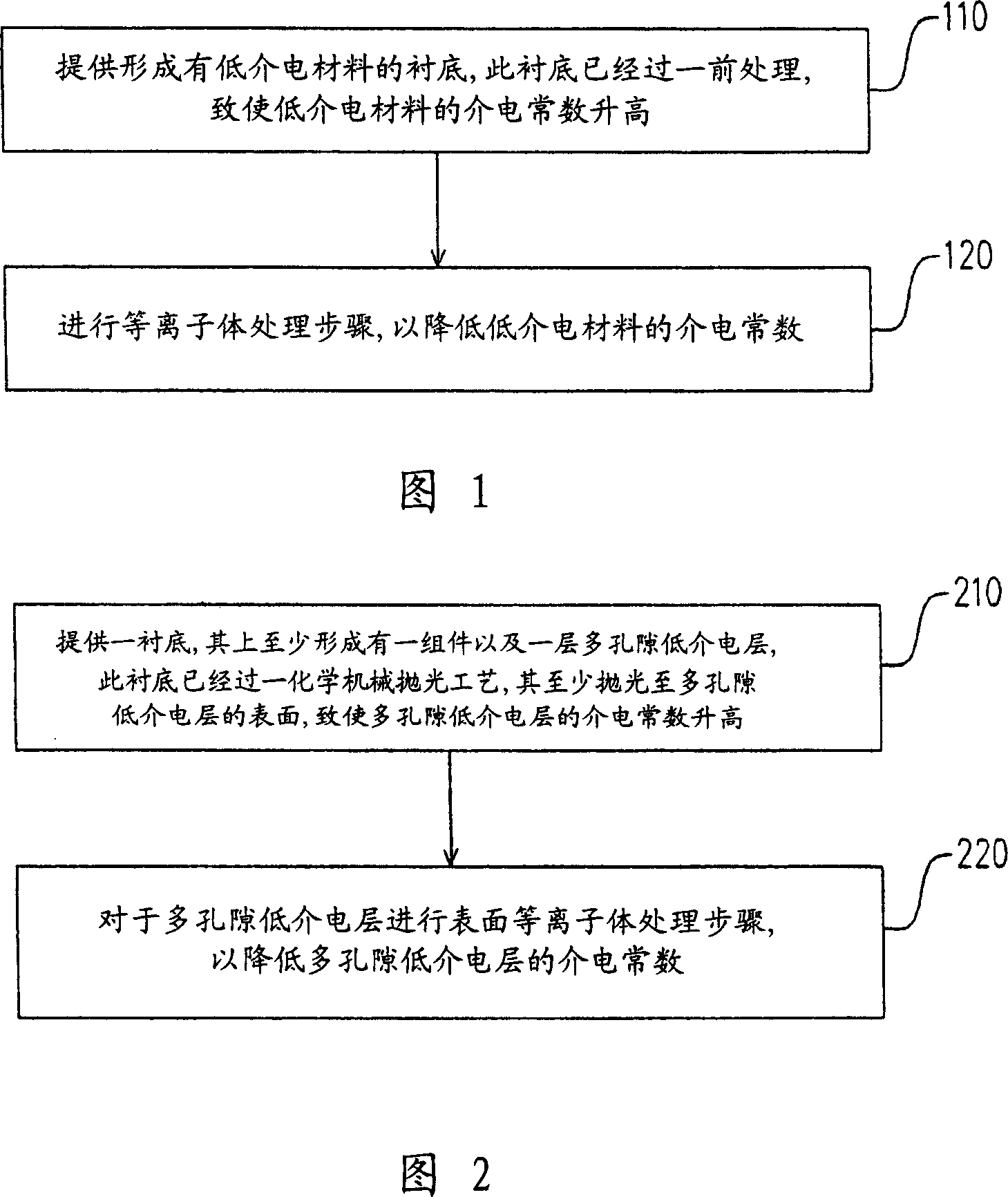
[0030] FIG. 1 is a flowchart illustrating a recovery method for low dielectric materials according to an embodiment of the present invention.

[0031] Referring to FIG. 1 , firstly, a substrate formed with a low-k material is provided, and the substrate has undergone a previous process to increase the dielectric constant of the low-k material (step 110 ). For example, elements such as MOS transistors or memories have been formed in the substrate, and the low dielectric material is, for example, a material constituting an inter-metal dielectric layer (Inter-Metal Dielectric, IMD). The low-dielectric material is, for example, a porous low-dielectric material, such as a pore-forming agent (porogen, whose composition is, for example, C x h y ) carbon doped oxide (Carbon DopedOxide, CDO), fluorinated amorphous carbon, Parylene AF4, PAE or Cyclotene, etc., and its dielectric constant is, for example, between 1.0 and 2.7. The method of forming the low dielectric material is, for ex...


PUM

PropertyMeasurementUnit
poweraaaaaaaaaa

Abstract

The invention relates to a method for returning low-dielectric material, used on the substrate with low-dielectric material. Wherein, said substrate has been processed, to increase the dielectric constant of low-dielectric material. And the invention is characterized in that it processes the low-dielectric material with plasma to reduce its dielectric constant.

Description

technical field [0001] The invention relates to a processing method for low dielectric materials, in particular to a recovery method for the dielectric constant of low dielectric materials. Background technique [0002] With the vigorous development of integrated circuits, in order to reduce the resistance-capacitance (RC) time lag caused by the interconnection and break through the bottleneck of operating speed, low-dielectric materials have become indispensable in today's semiconductor processes. missing important role. [0003] In order to make the dielectric constant of the low dielectric material closer to that of air (=1), the industry has developed low dielectric materials with many nanometer or sub-nanometer pores. However, this porous low-k dielectric material tends to absorb moisture, gas, or other pollutants after etching, ashing, solvent cleaning, or chemical-mechanical polishing processes, resulting in an increase in its dielectric constant and a change in its ...

Claims


Application Information

Patent Timeline
Patent Type & Authority Applications(China)
IPC IPC(8): H01L21/3105H01L21/4757
Inventor 陈美玲陈哲明赖国智苏文杰
Owner UNITED MICROELECTRONICS CORP
Why Eureka
Try Eureka